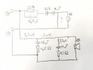
I posted it in 3 page. Post #53. I taked it from my pair.Does anyone have a schematic of the crossover for the Studio 630?
Here it is again. Cant measure inductance of coil in hipass filter. It probably arond 0.24mH

I posted it in 3 page. Post #53. I taked it from my pair.Does anyone have a schematic of the crossover for the Studio 630?
I posted it in 3 page. Post #53. I taked it from my pair.
Here it is again. Cant measure inductance of coil in hipass filter. It probably arond 0.24mH
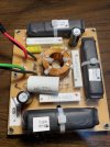
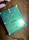
I did remove the the crossover board (pics included) and I couldn't see any visible traces between all of the parts. Maybe I'm missing something or don't know how to read the back of the board.The traces are on other side of the board. Have to unscrew it.
Guys, look at that DI curve! Look at the normalized horizontal polar! If you have access to EQ, it's going to be hard to find a better sounding speaker @ $350 per pair. We have to keep things in context of price here....

JBL Studio 630 6.5" 2-way Bookshelf Loudspeaker (Pair)Wood
JBL Studio 630 6.5" 2-way Bookshelf Loudspeaker (Pair) High definition imaging for high fidelity sound.For those searching for a home audio speaker system that goes above and beyond what they’ve ever heard, seek no further: The new JBL Studio 6 speaker system is everything your inner audiophile...www.safeandsoundhq.com
The large green"pads" that have solder points on them are the traces. They are just large to keep resistance low and to handle the high current. They are coated with a protective coating that is green. One slightly disturbing thing is the long wire ends of one of the components that have not been clipped off. You wouldn't want them to short to the other traces (the coating may lower the chance of that happening). I have the 630's as well, so I'll be interested in what you do.I did remove the the crossover board (pics included) and I couldn't see any visible traces between all of the parts. Maybe I'm missing something or don't know how to read the back of the board.
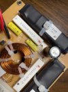
Ignore the Bevenbi cap because it didn't come with my speakers. I swapped mine out for testing purposes.
The large green"pads" that have solder points on them are the traces. They are just large to keep resistance low and to handle the high current. They are coated with a protective coating that is green. One slightly disturbing thing is the long wire ends of one of the components that have not been clipped off. You wouldn't want them to short to the other traces (the coating may lower the chance of that happening). I have the 630's as well, so I'll be interested in what you do.
")
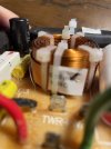
Hi Dan. The traces are the places the solder points are. They are more like "islands" in this case but serve the same purpose as the thin traces you were expecting. The area inside the red outline is the trace, for instance.Hi Jeff!
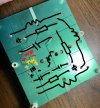
Yeah, I know where the solder points are, but I'm not seeing the "traces" that show the connection flow with other components. When I think of traces I think of clearly marked traces (see attached pic) that can easily be mapped out. I don't see that with this board at all. Maybe someone can take my picture and draw lines to show where the traces are because I don't see them. Maybe I'm blind?
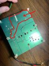
I'm currently in the testing phase that's why the long wire leads haven't been clipped off.
You can actually see the value in the picture from post #79, it's 0.5mHCant measure inductance of coil in hipass filter. It probably arond 0.24mH
Thank you so much for the schematic! The 750nF and 510nF caps are incorrectly marked on your drawing. 1nF is equal to 1/1,000,000mF so they would actually be 750,000nF and 510,000nF. Thanks again for your work!You can actually see the value in the picture from post #79, it's 0.5mH
I'm wondering if the low sensitivity in the midrange is a driver issue or if it's caused by the crossover.
View attachment 365639
Correct, however the cap is marked as 0.75uF which would be 0.00075mF or 750nF.1nF is equal to 1/1,000,000mF
Thank you, my mistake.Correct, however the cap is marked as 0.75uF which would be 0.00075mF or 750nF.
I would use uF to avoid confusion, but VituixCAD switches the units automatically
The large green"pads" that have solder points on them are the traces. They are just large to keep resistance low and to handle the high current. They are coated with a protective coating that is green. One slightly disturbing thing is the long wire ends of one of the components that have not been clipped off. You wouldn't want them to short to the other traces (the coating may lower the chance of that happening). I have the 630's as well, so I'll be interested in what you do.
As I told Jeff the reason why the leads haven't been clipped off is because I'm still in the testing phase. I'm testing and measuring different caps. I'm not going to clip the leads until its final. Sorry, but that's what I do.Exactly. Those green islands ARE the traces. They are much thicker than the little lines you often see on circuit boards because there is a lot more current (amps) going through them than in, for example, the traces between a CPU and memory chips, where the current is milli-amps or even micro-amps.
Also, yes, those leads not being clipped off is really, really sloppy production.
@dan87951, you should clip those off with wire cutters so that they only stick out a couple of millimeters (like the other leads that were properly clipped off).
Edit to add: After looking closer, that appears to be the big cap C5. If you look at the top of the board, you see that there really isn't enough room for C5 to be installed cleanly because the air core inductor L4 is too big for the space it was allotted. Sloppy work there. Either the CAD model for the inductor is wrong or they switched inductors to a slightly bigger one and didn't go back and update the board layout.
In any case, yeah, clip those long leads to be shorter.