This is a quick overview of how class D amplifiers operate. Note the “D” does not mean “digital”; it is simply the next letter in order as standards bodies enumerated amplifier types (A, B, C, D, E, F, G, H, I, etc.) It takes an analog, not digital, input and produces a pulse width modulated (PWM) output. I apologize in advance for the length.
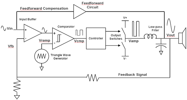
The figure below is a simplified schematic diagram of a class D amplifier. It is a rather busy diagram, so we’ll step through each piece from input to output. First the input signal, Vin, is applied to the input buffer (shown as an operational amplifier, opamp). The negative input of the opamp receives the feedback signal (Vfb) from the output (Vout). The output of the buffer is the difference between these two signals, providing a modified signal to the rest of the amplifier. The feedback signal allows the amplifier to correct any errors at the output, improving linearity (e.g. lowering distortion) and stabilizing the circuit so part variations, power supply and temperature changes, and other effects do not reduce performance. In the real world perfection is hard to find, so the output will not be perfect even with feedback, but it can get pretty close as Amir’s measurements have shown.
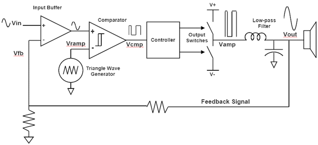
After the buffer is a comparator, a circuit that outputs a “high” if the (+) input is above the (-) input and a “low” otherwise. The (-) input is the comparator’s threshold voltage. This converts the input from a purely analog signal to one that is quantized (sampled) in amplitude though not in time. Almost but not quite a true digital signal, which is quantized in time and amplitude. A comparator with a clocked latch after it is a basic building block for an analog-to-digital convert (ADC). This is not an ADC. The other input to the comparator is a triangle wave; more about that shortly.
The comparator’s output (Vcmp) is applied to a controller. This is usually a logic circuit and voltage amplifier that drives the output switches. The controller can be complicated, but its basic job is to turn on either the high or the low switch, and never both at the same time! That would short the power rails through the switches, increasing power, heat, and chances of blowing up the amplifier.
The switches connect the unfiltered output (Vamp) to either the positive (V+) or negative (V-) power supply rail. Power is expended mainly as the signal is switched from high to low and back and the filter plus load (speaker) is charged; when the switches are static, little power is needed, as the signal is supplied from the output filter. That is the key to the high efficiency of a class D amplifier. There is no standing bias current in the output devices as in a class A or class AB amplifier. A push-pull class A amp has full current flowing all the time and is at best 50% efficient. A class AB amplifier reduces the current by only supplying current as needed to drive the load with minimal standing (constant) current just to cover the “gap” when the signal transitions from top and bottom devices. A class AB can achieve about 67% efficiency. By eliminating standing current, a class D amplifier can achieve 90% or higher efficiency, meaning much lower average power and much less power wasted as heat.
The switching rate is usually well above the audio band, perhaps 100 kHz to 1 MHz. That means no in-band power supply noise, but also adds very high frequency noise at the output. There is also a small “dead zone”, a time during which neither switch is on, thus higher switching frequency makes the dead zone as short as possible so it does not affect the output signal. The output low-pass filter is to get rid of all the high-frequency energy and deliver a smooth analog waveform to the speaker.
The triangle generator is what creates the high-frequency PWM signal to drive the switches. To see how it modulates the signal, consider replacing it with a DC source (a battery). If Vdc is 0 V, then the output is a square wave at the signal frequency. As you raise or lower the DC voltage, the period remains the same, but the pulse width changes since only part of the signal is above or below the threshold.

The period of the comparator’s output is the same as the input signal’s (same fundamental frequency) but the pulse width changes. Since you only have two levels (high and low), it is like a one-bit DAC without oversampling, and you would not be able to filter output. Not only is the switching rate too low, but it effectively varies with the signal, so you are just turning your input into a pulse train at the same frequency. Hardly useful for this application. By applying a high-frequency triangle wave, the pulses can be made much narrower, and the comparator’s output frequency is modulated to a much higher frequency. This allows the pulses to be filtered to create a smooth (analog) output signal.
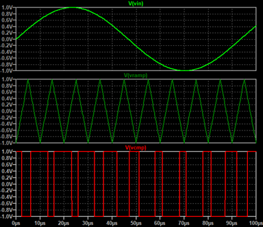
Here is a picture showing some of the waveforms inside the amplifier. The input at the top is a ~10 kHz sine wave. The triangle generator is producing a 100 kHz signal as shown in the middle. The bottom plot shows the comparator’s output. It creates a pulse train similar to that shown with a DC reference, but now the pulse train produces much higher-frequency pulses. Notice the high pulses are still generally longer as the input signal is higher, and shorter as the input signal drops below 0 V, but the pulses occur and a much higher rate. Now a simple filter can remove the high-frequency switching noise to create a smooth analog output.
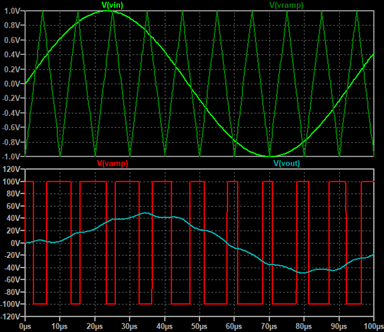
Moving on, the plots below show the input and triangle wave in the upper plot, and the output before and after the output filter in the lower plot. For the particular circuit simulated, the gain is set to produce ~100 Vpp for a 2 Vpp input using +/-100 V power supply rails. The Vamp signal looks exactly like the Vcmp signal as expected but scaled to the output level (+/-100 V instead of +/-1 V). At this scale you cannot see any dead zone in the output; like any decent design, it is as small as practical and invisible by eye. The ripples in the output signal Vout are because this amplifier is designed to operate at 500 kHz. I slowed it down to make it easier to see the switching waveforms, but that means the feedback and filter circuits are not adequately reducing switching noise at the output since they were designed for higher a switching frequency.
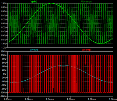
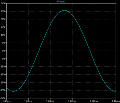
Here is the picture for the same 10 kHz input signal but switching at 500 kHz as designed. It is harder to see the triangle waves and distinguish the pulse shaping (width modulation) at the higher rate. The output signal is much smoother as seen in the next plot of just the output signal.
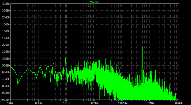
Finally here is an FFT (frequency plot) of the output signal. There are some low-frequency artifacts of the simulation and FFT resolution, plus some mixing products from the signal and switching frequencies, but the overall dynamic range is about 65 dB. This is an idealized design but also is not particularly optimized for performance – I just did enough to get it stable. The output filter rolls off over about 20 kHz, but you can clearly see the 500 kHz switching frequency tone about 50 dB below the output signal, then harmonics falling off above that. I could take more points and optimize the design for better performance but hopefully this shows enough to see generally how a class D amplifier works.
A word about the feedback circuit: making this stable means keeping the delay through the amp low enough and switching frequency high enough that the amp circuitry and output low-pass filter does not add too much phase shift. That was one of the biggest problems with early designs; the switching frequency was fairly low, so the feedback circuit (and output filter) had to roll off just above the audio band, and that caused a lot of phase shift in the audio band itself. There was little loop gain to reduce the distortion of higher-frequency audio signals and to ensure amplifier stability with complex loads (like many speakers). Too much phase shift and the feedback would be in phase with the input, adding instead of subtracting (positive feedback), and you have built an oscillator. A very powerful, speaker-eating oscillator. Switching frequencies have gotten much higher so this circuit can work well and is, I suspect, still the main compensation network for most of today's amplifiers.
Adding feedforward compensation is more prevalent today, at least in the very few schematics I have seen (remember this is not my day job). In this scheme some of the input signal is "fed forward" to the output to help bypass the switching stages and output filter. The feedforward circuit may include a low-power class A or AB amplifier that handles not only error correction but also provides most of the output for low-level signals. You must align the phase of the feed-forward circuit to the main signal path, of course, to add the right amount of feedforward compensation at the right time. Again, I do not know, but suspect many modern class D audio amplifiers are using this sort of approach. Some call it a hybrid design due to the class A/AB output driver.
Other schemes put multiple switches in parallel, but staggered in time, so the effective switching rate is much higher, use more complex generators to create PWM/PFM and other output signals, and so forth. Too complicated for one post.
HTH - Don
The figure below is a simplified schematic diagram of a class D amplifier. It is a rather busy diagram, so we’ll step through each piece from input to output. First the input signal, Vin, is applied to the input buffer (shown as an operational amplifier, opamp). The negative input of the opamp receives the feedback signal (Vfb) from the output (Vout). The output of the buffer is the difference between these two signals, providing a modified signal to the rest of the amplifier. The feedback signal allows the amplifier to correct any errors at the output, improving linearity (e.g. lowering distortion) and stabilizing the circuit so part variations, power supply and temperature changes, and other effects do not reduce performance. In the real world perfection is hard to find, so the output will not be perfect even with feedback, but it can get pretty close as Amir’s measurements have shown.
After the buffer is a comparator, a circuit that outputs a “high” if the (+) input is above the (-) input and a “low” otherwise. The (-) input is the comparator’s threshold voltage. This converts the input from a purely analog signal to one that is quantized (sampled) in amplitude though not in time. Almost but not quite a true digital signal, which is quantized in time and amplitude. A comparator with a clocked latch after it is a basic building block for an analog-to-digital convert (ADC). This is not an ADC. The other input to the comparator is a triangle wave; more about that shortly.
The comparator’s output (Vcmp) is applied to a controller. This is usually a logic circuit and voltage amplifier that drives the output switches. The controller can be complicated, but its basic job is to turn on either the high or the low switch, and never both at the same time! That would short the power rails through the switches, increasing power, heat, and chances of blowing up the amplifier.
The switches connect the unfiltered output (Vamp) to either the positive (V+) or negative (V-) power supply rail. Power is expended mainly as the signal is switched from high to low and back and the filter plus load (speaker) is charged; when the switches are static, little power is needed, as the signal is supplied from the output filter. That is the key to the high efficiency of a class D amplifier. There is no standing bias current in the output devices as in a class A or class AB amplifier. A push-pull class A amp has full current flowing all the time and is at best 50% efficient. A class AB amplifier reduces the current by only supplying current as needed to drive the load with minimal standing (constant) current just to cover the “gap” when the signal transitions from top and bottom devices. A class AB can achieve about 67% efficiency. By eliminating standing current, a class D amplifier can achieve 90% or higher efficiency, meaning much lower average power and much less power wasted as heat.
The switching rate is usually well above the audio band, perhaps 100 kHz to 1 MHz. That means no in-band power supply noise, but also adds very high frequency noise at the output. There is also a small “dead zone”, a time during which neither switch is on, thus higher switching frequency makes the dead zone as short as possible so it does not affect the output signal. The output low-pass filter is to get rid of all the high-frequency energy and deliver a smooth analog waveform to the speaker.
The triangle generator is what creates the high-frequency PWM signal to drive the switches. To see how it modulates the signal, consider replacing it with a DC source (a battery). If Vdc is 0 V, then the output is a square wave at the signal frequency. As you raise or lower the DC voltage, the period remains the same, but the pulse width changes since only part of the signal is above or below the threshold.
The period of the comparator’s output is the same as the input signal’s (same fundamental frequency) but the pulse width changes. Since you only have two levels (high and low), it is like a one-bit DAC without oversampling, and you would not be able to filter output. Not only is the switching rate too low, but it effectively varies with the signal, so you are just turning your input into a pulse train at the same frequency. Hardly useful for this application. By applying a high-frequency triangle wave, the pulses can be made much narrower, and the comparator’s output frequency is modulated to a much higher frequency. This allows the pulses to be filtered to create a smooth (analog) output signal.
Here is a picture showing some of the waveforms inside the amplifier. The input at the top is a ~10 kHz sine wave. The triangle generator is producing a 100 kHz signal as shown in the middle. The bottom plot shows the comparator’s output. It creates a pulse train similar to that shown with a DC reference, but now the pulse train produces much higher-frequency pulses. Notice the high pulses are still generally longer as the input signal is higher, and shorter as the input signal drops below 0 V, but the pulses occur and a much higher rate. Now a simple filter can remove the high-frequency switching noise to create a smooth analog output.
Moving on, the plots below show the input and triangle wave in the upper plot, and the output before and after the output filter in the lower plot. For the particular circuit simulated, the gain is set to produce ~100 Vpp for a 2 Vpp input using +/-100 V power supply rails. The Vamp signal looks exactly like the Vcmp signal as expected but scaled to the output level (+/-100 V instead of +/-1 V). At this scale you cannot see any dead zone in the output; like any decent design, it is as small as practical and invisible by eye. The ripples in the output signal Vout are because this amplifier is designed to operate at 500 kHz. I slowed it down to make it easier to see the switching waveforms, but that means the feedback and filter circuits are not adequately reducing switching noise at the output since they were designed for higher a switching frequency.
Here is the picture for the same 10 kHz input signal but switching at 500 kHz as designed. It is harder to see the triangle waves and distinguish the pulse shaping (width modulation) at the higher rate. The output signal is much smoother as seen in the next plot of just the output signal.
Finally here is an FFT (frequency plot) of the output signal. There are some low-frequency artifacts of the simulation and FFT resolution, plus some mixing products from the signal and switching frequencies, but the overall dynamic range is about 65 dB. This is an idealized design but also is not particularly optimized for performance – I just did enough to get it stable. The output filter rolls off over about 20 kHz, but you can clearly see the 500 kHz switching frequency tone about 50 dB below the output signal, then harmonics falling off above that. I could take more points and optimize the design for better performance but hopefully this shows enough to see generally how a class D amplifier works.
A word about the feedback circuit: making this stable means keeping the delay through the amp low enough and switching frequency high enough that the amp circuitry and output low-pass filter does not add too much phase shift. That was one of the biggest problems with early designs; the switching frequency was fairly low, so the feedback circuit (and output filter) had to roll off just above the audio band, and that caused a lot of phase shift in the audio band itself. There was little loop gain to reduce the distortion of higher-frequency audio signals and to ensure amplifier stability with complex loads (like many speakers). Too much phase shift and the feedback would be in phase with the input, adding instead of subtracting (positive feedback), and you have built an oscillator. A very powerful, speaker-eating oscillator. Switching frequencies have gotten much higher so this circuit can work well and is, I suspect, still the main compensation network for most of today's amplifiers.
Adding feedforward compensation is more prevalent today, at least in the very few schematics I have seen (remember this is not my day job). In this scheme some of the input signal is "fed forward" to the output to help bypass the switching stages and output filter. The feedforward circuit may include a low-power class A or AB amplifier that handles not only error correction but also provides most of the output for low-level signals. You must align the phase of the feed-forward circuit to the main signal path, of course, to add the right amount of feedforward compensation at the right time. Again, I do not know, but suspect many modern class D audio amplifiers are using this sort of approach. Some call it a hybrid design due to the class A/AB output driver.
Other schemes put multiple switches in parallel, but staggered in time, so the effective switching rate is much higher, use more complex generators to create PWM/PFM and other output signals, and so forth. Too complicated for one post.
HTH - Don
Last edited:
