I have a feeling this got a bit lost in the shuffle, over in the audio interface section. I got curious why EIN in this interface was seemingly so bad (-108ish dBu flat).
First of all, my UR12 Black looks the same as any other UR12 inside, see e.g.
Reverse-engineering with associated discussion starts here:

 www.audiosciencereview.com
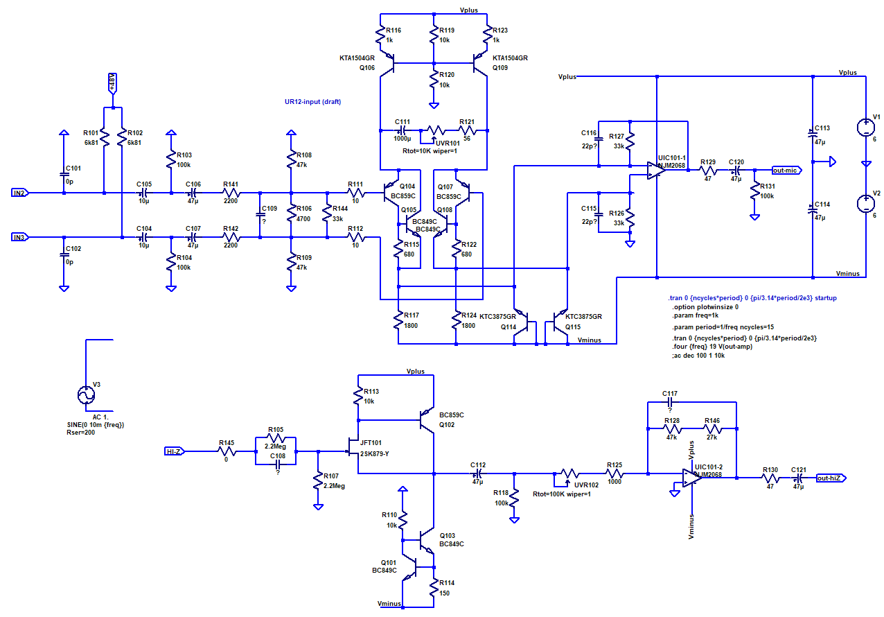
The fruits of my labor:

It's a basically decent circuit but the attenuation and noise introduced by two 2k2 series resistors totally ruins noise performance, even before taking in consideration the hundreds of ohms of rbb' in the BC859 input transistors.
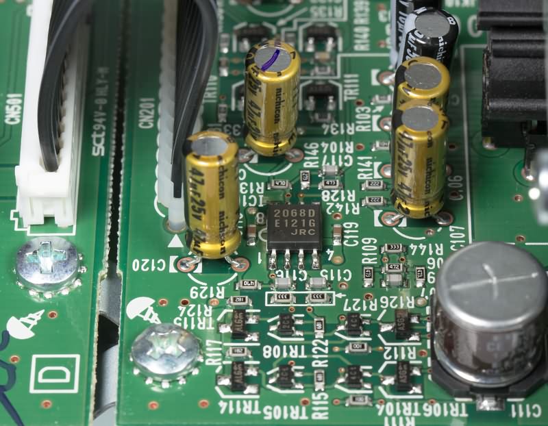
The question of how to salvage this while providing adequate protection against the Phantom Menace still stands. There's basically no easy access to the supplies up until the point at which the signal surfaces at the PCB top side just prior to R111/112 at the input stage (a slightly crowded area), as the PCB seems to be something like a 3- or 4-layer board. This picture from the iXBT review depicts the exact area:

You could get access to V- at TR114/115, though annoyingly all the resistors going to V+ are on the underside again.
The bridge diodes to V- could be mounted sticking up from R111/112 which would minimize their effect as they are normally nonconductive. As for the V+ side, well, if push comes to shove one may have to run a wire all the way around the board at due distance (possibly even a tiny coax). None of this strikes me as particularly mechanically robust.
Am I correct in assuming that TR114/115 are already performing the job of clamping diodes D5/D6 proposed by Bortoni and Kirkwood?
If you are going to leave the BC859s as-is, I suppose 47-100 ohms in parallel to or instead of R141/142 wouldn't hurt much while providing better protection. Not a good spot to solder in, unless you were going to rectify this coupling capacitor mess as well. (I suppose they didn't trust the 10µ/50s alone but didn't have anything better so included some 47µ/25s in series. Dumb. If you have some good quality, low-leakage 22µ-47µ/63s you could fit instead of the 10µ/50s, I would suggest doing so. ESR is not critical but leakage and matching are. The old 22µs can then be replaced by jumpers, and you'll have great access to the two resistors. Some increase in capacitance is going to be necessary as input impedance would be roughly halved after the fix.)
As far as input transistor replacements for further EIN improvements post-fix are concerned, you could actually do worse than some MMBT3906s, as silly as that sounds. 2SA1163 also looks like a fairly promising candidate (rbb' seems to be in the 40s, and beta is quite high).
First of all, my UR12 Black looks the same as any other UR12 inside, see e.g.
Reverse-engineering with associated discussion starts here:

More Steinberg UR12 Black measurements
(Initial observations start in this thread, with more on input noise here.) RCA L --> XLR mic in (nominal Zin = 4k, Zout = 600R). -12dBFS at max output + min input gain becomes -3.49 dBFS in. The difference between min and max gain settings is 43 dB. (Spec: Gain 10-54 dB, so we're only 1 dB off...
 www.audiosciencereview.com
The fruits of my labor:
It's a basically decent circuit but the attenuation and noise introduced by two 2k2 series resistors totally ruins noise performance, even before taking in consideration the hundreds of ohms of rbb' in the BC859 input transistors.
The question of how to salvage this while providing adequate protection against the Phantom Menace still stands. There's basically no easy access to the supplies up until the point at which the signal surfaces at the PCB top side just prior to R111/112 at the input stage (a slightly crowded area), as the PCB seems to be something like a 3- or 4-layer board. This picture from the iXBT review depicts the exact area:

You could get access to V- at TR114/115, though annoyingly all the resistors going to V+ are on the underside again.
The bridge diodes to V- could be mounted sticking up from R111/112 which would minimize their effect as they are normally nonconductive. As for the V+ side, well, if push comes to shove one may have to run a wire all the way around the board at due distance (possibly even a tiny coax). None of this strikes me as particularly mechanically robust.
Am I correct in assuming that TR114/115 are already performing the job of clamping diodes D5/D6 proposed by Bortoni and Kirkwood?
If you are going to leave the BC859s as-is, I suppose 47-100 ohms in parallel to or instead of R141/142 wouldn't hurt much while providing better protection. Not a good spot to solder in, unless you were going to rectify this coupling capacitor mess as well. (I suppose they didn't trust the 10µ/50s alone but didn't have anything better so included some 47µ/25s in series. Dumb. If you have some good quality, low-leakage 22µ-47µ/63s you could fit instead of the 10µ/50s, I would suggest doing so. ESR is not critical but leakage and matching are. The old 22µs can then be replaced by jumpers, and you'll have great access to the two resistors. Some increase in capacitance is going to be necessary as input impedance would be roughly halved after the fix.)
As far as input transistor replacements for further EIN improvements post-fix are concerned, you could actually do worse than some MMBT3906s, as silly as that sounds. 2SA1163 also looks like a fairly promising candidate (rbb' seems to be in the 40s, and beta is quite high).
