• WANTED: Happy members who like to discuss audio and other topics related to our interest. Desire to learn and share knowledge of science required. There are many reviews of audio hardware and expert members to help answer your questions. Click here to have your audio equipment measured for free!

JBL VRX932LAP Amp - Power flickering on and off in rapid succession

beavernuggetz

Member
Joined
Sep 21, 2023
Messages
36
Likes
2
Hello everyone,

I am working on 4 of these JBL amps for a DJ friend of mine. The initial issue was of course some sort of power surge fried some components on the board. This is the first one I'm working on.

Pictures and videos can be seen here @ MyGoogleDrive. If this is not allowed, please let me know.

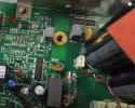
On the bottom, the GB20B60PD1 IGBTs were blown to pieces and on top there were lots of SMD components which are near the IGBTs were also shorted.

I gathered the list of dead components and ordered replacements from DigiKey and Mouser.
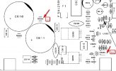
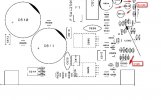
Couple of issues with the parts. First. the GB20B60PD1 IGBTs are no longer manufactured so watched a few YouTube videos where a guy used IKP20N60TXKSA1 instead; ordered them since the specs match closely with the originals. Second, there are 4 high voltage transistors labelled MPSW42 (Q607-610; see schematic attachment) which are no longer manufactured, used MPSA42 instead because they are nearly identical. The rest of the parts were in stock including TL494, FAN7380, J1 & K1 transistors, etc.

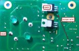
Once all the parts were replaced but without having the TL494 (Switching Controller) & FAN7380MX (High-Side Gate Driver IC) connected, turned the amp on, measured 17 volts between SMD resistor R604 and the U1J diode as shown in one of the videos. Believing the voltage was okay, soldered the remaining components but the issue described in the first video came up; when powering up the amp, the front LEDs come on and after about 20 seconds the power light (blue one) starts blinking frequently and a clicking noise can be heard. There are no shorts because the amp is connected to a lamp current limiter; have tried connecting it directly to an outlet with the same result.

Does anyone know what this symptom means and what could be the cause? Could it be the parts which had to be substituted causing this?

All feedback is welcome and will be highly appreciated.
 

Attachments

  • crown_jbl_vrx932_mainboard_prx_vrx_pwa_dpc2_sch.pdf
    241.6 KB · Views: 90

AnalogSteph

Major Contributor
Joined
Nov 6, 2018
Messages
3,395
Likes
3,344
Location
.de
Believing the voltage was okay, soldered the remaining components but the issue described in the first video came up; when powering up the amp, the front LEDs come on and after about 20 seconds the power light (blue one) starts blinking frequently and a clicking noise can be heard.
And the clicking is basically in sync with the blinking?

The good news is that the circuit appears to basically be working, the bad news is that +5VD collapses even trying to sustain the relay current.

You've probably had to change the 5A fuse for 1/2VBULK?

First off, please verify that +/-VCC are actually stable - TP601/603 vs. TP602. Likewise, check what +5VD is doing e.g. at the 3904 (Q1) or the 74HC74 (U2). It is unclear what actually provides the LED drive signal that comes in via J1, in any case check what that's doing at R5 if everything else is stable.
 
OP
B

beavernuggetz

Member
Joined
Sep 21, 2023
Messages
36
Likes
2
Hey @AnalogSteph, thank you for taking the time to respond.
I actually figured it out, the parts worked fine and the amp was simply going into protection mode because the PCB was not bolted down into the chassis therefore the IGBTs were getting hot.

I do have another one which is giving me a hard time though. The 17 volts between SMD resistor R604 and the U1J diode is non-existent after replacing all the parts. I've traced power across the bridge rectifier which appears to be working normally but I'm lost where to check next. My knowledge is intermediate at best and to be honest reading schematics is not something I'm good at as of yet.

Any ideas how to trace voltage to figure out where it's dropping off?
 

AnalogSteph

Major Contributor
Joined
Nov 6, 2018
Messages
3,395
Likes
3,344
Location
.de
Stupid question, is everything about the unit working normally now? I'd hate to be chasing a "problem" where none actually exists.

I'm honestly not sure what exactly you are measuring there. Is it between the "ground" (SMPSREF) end of R604 and the cathode of either D609 and D610, i.e. the unregulated voltage input to the +15V CONTROL regulator? I am pretty sure that without this voltage, the unit would not even work. Like, at all. It feeds both the TL494 and the gate driver IC. You would have zero power supply output.

BTW, I hope you are either very cautious measuring on the primary side or better yet, using an isolation transformer to run the unit.
 
OP
B

beavernuggetz

Member
Joined
Sep 21, 2023
Messages
36
Likes
2
@AnalogSteph my apologies for not being more clear during the last post.

The issue now is with a separate amp which is the exact same model; the first one is done and functional.

This video makes it more clear as to what I mean about measuring for the 17 volts. On the first amp, the 17 volts were there without the TL494 as well as the gate driver IC being soldered; the whole idea is to verify proper voltage first before soldering these 2 chips & powering up the amp for safety reasons and to prevent the IGBTs as well as the nearby SMD components from getting fried due to improper voltage. I am indeed getting 0 volts on this second amp between those 2 points even after replacing the same parts as the first one, so my question is about trying to figure out where the voltage is dropping or which components are responsible for providing such voltage.

It seems the schematics attached in the original post does not match the amp in regards to some component labels.

Yes, the amp gets the power from a series lamp or an isolation transformer; got both.

I own good multimeters and oscilloscope but lack the proper knowledge for the latter.

Find attached images showing where I am measuring for the 17 volts just as described in the video.

Appreciate your time and willingness to help by the way.
 

Attachments

  • 2023-09-28_095015.jpg
    2023-09-28_095015.jpg
    106.1 KB · Views: 64
  • 2023-09-28_095455.jpg
    2023-09-28_095455.jpg
    90.5 KB · Views: 64
OP
B

beavernuggetz

Member
Joined
Sep 21, 2023
Messages
36
Likes
2
Also not hearing any clicking from the relay so will start there to see if it's faulty.
 

AnalogSteph

Major Contributor
Joined
Nov 6, 2018
Messages
3,395
Likes
3,344
Location
.de
Sorry for the long delay. It seems you are measuring between +15V CONTROL and SMPSREF. OK, let's see where that voltage comes from.

Here's the circuitry in question:
vrx932-15vcontrol.png


Measure between your existing R604 test point (SMPSREF) and either end of R642. What do you get? You ought to be seeing 29ish V, and I suspect there's nothing on at least one end.

The way this circuit works is quite simple:

Final regulation is done by a simple zener regulator with 3 paralleled MPSW42s (Q607-9, combined via R637-8-9) as emitter followers and a 17V zener (D607) at the base that is being supplied by R640/641. (top left)

The regulator in itself is fed via R642/C634 from either of two sources, whichever puts out the higher voltage:
1. If the power supply is not running, the zener regulator around Q610 is active (bottom). 30V zener D606 is fed via series resistors R656-R655-R644 (255k each) from VBULK, which is the full rectified DC voltage across both primary capacitors C610 + C611 (320-ish V?). Emitter follower Q610 is being supplied from VPRI, which is VBULK tapped off via a 24k/75k voltage divider R610/R612. Assuming VBULK is fine, check for open resistors (particularly the 3 x 255k resistor chain and R610), open Q610 and shorted zener D606.
2. Once the power supply is running, an auxiliary transformer winding comes into play (top right).
a) Its voltage is being rectified / smoothed via D608 / C635 and turns on Q611 (bottom right), which pulls D606 voltage down to near 0 V. Q610 voltage follows (that's why it's called a voltage follower, duh). Make sure Q611 is not shorted C-E.
b) It also takes over the supply via D610 - R642 - C634 (rectifier / smoothing). D609 prevents backfeeding into Q610, which now is conducting zero current though it still has to sustain a fair bit of voltage.

Note, you'll probably want to improve heatsinking when using MPSA42 instead of MPSW42, especially Q607-9. You can buy TO-92 heatsinks, but DIY may also be an option.
 
Last edited:
OP
B

beavernuggetz

Member
Joined
Sep 21, 2023
Messages
36
Likes
2
Wow, your ability to read and understand schematics is amazing! Wish I had someone like you around to learn and pick your brains.

Will perform the tests you suggested later and report back with my findings. Thanks for the heatsink warning as well.

Wanted to express my gratitude as well for taking the time to explain things in so much detail.
 
OP
B

beavernuggetz

Member
Joined
Sep 21, 2023
Messages
36
Likes
2
Sorry it took me a few days to get back to you, @AnalogSteph but here are my findings thus far.

Unfortunately there are no obvious shorts or defective components as the ones you mentioned test okay and the readings are the same as in the working amp.

Where do I go from here? Should I de-solder the components you suggested first before testing? Thus far I'm simply testing them on the PCB and comparing the readings with the working unit.

Here is a breakdown of the findings.

Q: Measure between your existing R604 test point (SMPSREF) and either end of R642. What do you get?

A: Absolutely nothing on either end of this 10 Ohm resistor.

Q: Assuming VBULK is fine, check for open resistors (particularly the 3 x 255k resistor chain and R610), open Q610 and shorted Zener D606.

A: VBULK (D606 + R656-R655-R644) all test okay. R610 has been replaced and the 3 x 255K resistor chain test within specs.

R656-R655-R644 (255k each) --- All 3 measure 255K just as the ones on the working amp.

C610 + C611 (320-ish V?) --- Yes, each show approximately 167 volts when measuring at R603 & R604.

30V Zener D606 --- Tests okay and it is not shorted; reads the same as the one on the working amp.

24k/75k voltage divider R610/R612 --- Both have been replaced.

Q610 --- Has been replaced.
 

AnalogSteph

Major Contributor
Joined
Nov 6, 2018
Messages
3,395
Likes
3,344
Location
.de
Huh. You must have a bad via or trace or something (lifted pad?).

What do you get for voltages at points throughout the 255k resistor chain and at the collector and emitter of Q610 (ref. SMPSREF)? If you say D606 reads the same as the one in the other amp, does that also apply to voltage in operation?

A shorted D610 would keep the circuit from working I would think, in case you haven't checked that.
 
Last edited:
OP
B

beavernuggetz

Member
Joined
Sep 21, 2023
Messages
36
Likes
2
Okay, did a bit more measuring and comparing values between the 2 amps.

I haven't tested voltages in those specific areas you mentioned but will tackle that next; I'm a bit worried about shorting components out but will have to just be careful.

D610 measures fine and is not shorted.

D606 - Where would I measure voltage? Across its legs or still by referencing SMPSREF?


Now, here are some differences spotted between the 2 amps in regards to some of the components.

D607 which is labelled 8X and is a 17v Zener diode according to your previous post. This one appears to be MMBZ5247B.
On the working board, the diode measures 0.735 voltage drop and on the non-working one it comes back with 0.440.

C664 which is labelled CD471K which is a '470 pF Safety X1 Y1 Capacitor' and is no longer manufactured.
On the working board, it measures 10.42nF and on the defective one it shows 0.553nF.

What are your thoughts on these 2 findings?
 

AnalogSteph

Major Contributor
Joined
Nov 6, 2018
Messages
3,395
Likes
3,344
Location
.de
I haven't tested voltages in those specific areas you mentioned but will tackle that next; I'm a bit worried about shorting components out but will have to just be careful.
It is best to solder a wire to SMPSREF and use a clip lead or something. Probing with two hands is just asking for trouble.
D606 - Where would I measure voltage? Across its legs or still by referencing SMPSREF?
The anode ought to be on SMPSREF anyway, so it should not matter. (If it does, there's a problem.)
D607 which is labelled 8X and is a 17v Zener diode according to your previous post. This one appears to be MMBZ5247B.
On the working board, the diode measures 0.735 voltage drop and on the non-working one it comes back with 0.440.
Was this measured in circuit or out of circuit? If the latter, possibly a leaky diode (may develop due to long-term heat stress). (What do you get in reverse?) If the former, possibly a leaky C600 or something.
C664 which is labelled CD471K which is a '470 pF Safety X1 Y1 Capacitor' and is no longer manufactured.
On the working board, it measures 10.42nF and on the defective one it shows 0.553nF.
This is in circuit, right?

Now it gets weird. 553 pF certainly seems right for a 470 pF part plus some parasitics. This is the only direct connection to chassis ground, anything else has to be indirectly via SMPSREF (C611-C666). So perhaps your SMPSREF is interrupted somewhere on its way back.

Can you verify that you have continuity from one end of C664 to SMPSREF? It should be going straight through the auxiliary winding (T601 2 --> 1 --> SMPSREF), I don't think that would have more than a few (dozen) ohms. Reverse meter leads to make sure D610/D608 are out of the picture.

T601 pin 1 should also be connected directly to the negative end of C611.
 
OP
B

beavernuggetz

Member
Joined
Sep 21, 2023
Messages
36
Likes
2
All measurements were done in circuit and without de-soldering components first. I've had a wire attached to SMPSREF this whole time and use a crocodile clip on that end to read voltages. I've messed up before by doing exactly what you mentioned; probing around with 2 hands hence the hesitation.

Using a microscope and the naked eye, I haven't been able to spot any damaged vias or traces thus far; have also followed the tracks checking for continuity and found no issues.

The anode (D606) ought to be on SMPSREF anyway, so it should not matter.
Indeed, it is directly connected with almost 0 resistance.

Can you verify that you have continuity from one end of C664 to SMPSREF?
Yes, there is almost 0 resistance between the 2 points.

T601 pin 1 should also be connected directly to the negative end of C611.
The first 2 pins (out of 6) on one side (the pins are directly across D600/K601) are directly connected.

What do you get for voltages at points throughout the 255k resistor chain and at the collector and emitter of Q610 (ref. SMPSREF)?
Absolutely nothing; 0 volts.

Reverse meter leads to make sure D610/D608 are out of the picture.
Done and it shows OL on both.

D607 ... possibly a leaky diode (may develop due to long-term heat stress). (What do you get in reverse?
In reverse it reads normal; OL. The only concern around this Diode is a dark spot on the top which does not show up on the one in the working amp; can provide a picture if you wish.

Now it gets weird. 553 pF certainly seems right for a 470 pF part plus some parasitics.
Seems the readings look good on the non-working amp as compared to the working one just going by the value of the capacitor (470 pF) alone.

As a matter of fact and using a thermal camera, the only heat spots on the board are R603 & R603 which are located on each side of C610 & C611. This is also the only spots where voltages can be read (close to 170 DC) and nowhere else.

Again, thank you very much for your help. Please let me know if there are any other areas where I could check for potential issues.
 
Last edited:

AnalogSteph

Major Contributor
Joined
Nov 6, 2018
Messages
3,395
Likes
3,344
Location
.de
What do you get for voltages at points throughout the 255k resistor chain and at the collector and emitter of Q610 (ref. SMPSREF)?
Absolutely nothing; 0 volts.
What the actual...?

Please verify that one side of R656 (the first of the 255ks), R610 (opposite from R612) and the + side of C610 (R603) are all connected. There has to be a break somewhere.

Likewise, SMPSREF at D606/D607 anode must go through to C611 (-)/R604.
As a matter of fact and using a thermal camera, the only heat spots on the board are R603 & R603 which are located on each side of C610 & C611. This is also the only spots where voltages can be read (close to 170 DC) and nowhere else.
So no voltage across R610-R612 either?

Maybe shorted Q605-606 have smoked one of the main VBULK / SMPSREF traces? Not sure what the routing is like, but they are somewhere in between C610/611 and the area that seems to have no juice whatsoever. A hairline crack in the board would be another option.
 
OP
B

beavernuggetz

Member
Joined
Sep 21, 2023
Messages
36
Likes
2
So no voltage across R610-R612 either?
Correct, there is nothing there either.

SMPSREF at D606/D607 anode must go through to C611 (-)/R604.
Yes, there is connectivity here.

Likewise, SMPSREF at D606/D607 anode must go through to C611 (-)/R604.
Yes, the connections are there.

Please verify that one side of R656 (the first of the 255ks), R610 (opposite from R612) and the + side of C610 (R603) are all connected. There has to be a break somewhere.
And here is where you hit the nail on the head.
There is continuity between R656 and R610; all normal in this area.
However, there is no connection between R610 and + side of C610 (R603); checked the working amp and the connection is present.

Here is a picture of the underside of the area in question, perhaps you can spot something I'm missing.
At this point, what are my options? Is running a wire between these 2 points an option? Perhaps it isn't as simple as all that.

Thanks again for all your help.
PS: Nice blog by the way.
 

Attachments

  • PXL_20231009_235227840.jpg
    PXL_20231009_235227840.jpg
    130 KB · Views: 52

AnalogSteph

Major Contributor
Joined
Nov 6, 2018
Messages
3,395
Likes
3,344
Location
.de
Here is a picture of the underside of the area in question, perhaps you can spot something I'm missing.
At this point, what are my options? Is running a wire between these 2 points an option?
Basically, yes. (With some precautions regarding insulation, that is, we are talking 330ish V DC after all.) I would still like to find a proverbial smoking gun. Hard to tell with just the underside, it appears to be a double-sided PCB. Ideally you would have perfectly aligned shots of both sides so both can be overlaid (one mirrored, obviously), but in this case you may be OK just following the fat trace from C610 as it makes its way to Q605 / C616 / C615 as well as turning the board over to follow things from R610 backwards, they obviously have to meet somewhere. Probe component legs along the way. Pay special attention to vias.

If it turns out to be a bad via, the standard fix is sticking a thin piece of bare wire through and soldering it on both sides. Enlarging the hole a bit manually with a tiny drill may be needed.
 
OP
B

beavernuggetz

Member
Joined
Sep 21, 2023
Messages
36
Likes
2
Checked vias and all appear to be connected using a multimeter as well as a really bright light to check for damaged tracks.

Here are some additional findings which may or may not be expected. These differences were discovered by comparing with the working amp.

  1. There is no connection between R610 and D01 Bridge Rectifier which is definitely getting power per earlier tests.
  2. R610 - No connection to SMPSREF.
  3. R610 - No connection to either C615 or C616.
  4. R612 - No connection to either C615 or C616.
  5. R610 - Has connection to Q605.

Don't believe it makes a difference but TL494 (Switching Controller) & FAN7380MX (High-Side Gate Driver IC) are not currently soldered to the board until the +17 volts are present at D605 just like in the video.
 

AnalogSteph

Major Contributor
Joined
Nov 6, 2018
Messages
3,395
Likes
3,344
Location
.de
Here are some additional findings which may or may not be expected. These differences were discovered by comparing with the working amp.

  1. There is no connection between R610 and D01 Bridge Rectifier which is definitely getting power per earlier tests.
  2. R610 - No connection to SMPSREF.
  3. R610 - No connection to either C615 or C616.
  4. R612 - No connection to either C615 or C616.
  5. R610 - Has connection to Q605.
Wait, the working amp does not have #5? 'cause it definitely should! That would explain the remaining "hiccups", as the startup supply probably doesn't have enough power for sustained operation.

#2 - R610 should not have a direct connection to SMPSREF, so that's correct (there's the 75k R612 in the way). R612 should though.

#1+#3+#5 lead me to believe that there is no connection between Q605 and C610 / rectifier either? That's odd, you'd think one would be able to spot any major breaks in this relatively stout trace. I can't see where it goes after C616 though, it's either behind Q605 or on the other side of the board. The fault has to be somewhere in that vicinity. Maybe a pad come off or a solder joint that's not flowed all the way through on Q605 or C616. Check that all the legs of Q605 are making it through to its pads. (It might even be something mean like the C616 leg having served as a fuse inside the board!)

Wherever component legs are serving as connections between both sides of the board, solder must flow through and make a proper connection to both pads, and both pads must obviously be attached to their respective traces. This is an area where things can very much go wrong during repairs, so it deserves corresponding scrutiny.

If you have some UV-curing solder mask or at least some nail polish at hand for repair, probing on traces after exposing a tiny bit would be an option.

#4 suggests that you have an additional break in the SMPSREF connection. That will need to be dealt with as well.
 
Last edited:
OP
B

beavernuggetz

Member
Joined
Sep 21, 2023
Messages
36
Likes
2
I'm back with some good and bad news.

After running a jumper (see attachment) using a thick enameled coated wire between those 2 points I know have some voltages at R610/R612 through hole resistors as well as the 255k array; it is 24 VDCs at both points. The bad news, the voltage at D605 is only 4 VDC instead of the expected ~17 with reference to SMPSREF.

Once I have a bit more time I'll come back with answers to some of your questions from above.

Thanks again for all your help.
 

Attachments

  • Jumper_Wire_0001.jpg
    Jumper_Wire_0001.jpg
    94.5 KB · Views: 35
  • Voltages_001.jpg
    Voltages_001.jpg
    132.7 KB · Views: 45

AnalogSteph

Major Contributor
Joined
Nov 6, 2018
Messages
3,395
Likes
3,344
Location
.de
Makes sense if you still have a duff SMPSREF connection. That's probably elevated at R612 vs. C611 now.

Thankfully there's not exactly a shortage of SMPSREF traces and solder joints. From what I know I would add another jumper wire as follows:
JUMPER_WIRE_0002.jpg

Please verify that things are as shown.

What we want is VBULK -- R610 -- (VPRI branching off to 255k) -- R612 -- SMPSREF.

You must know for sure which two terminals of R610/612 are connected, or else there could be a big smoke show if you mistakenly attach both of your jumper wires to that node.

The VBULK trace that you have attached your jumper wire to at C615 looks a bit wimpy. I might have proceeded around Q605 to that nice big C616 solder joint slightly obscured by the Q605 tab. I think it'll work though.
 
Top Bottom