OP
syn08
Senior Member
- Thread Starter
- #41
No, nothing major indeed. Lots of lessons learned about optimal layout (extremely important), distortion correction in the ESS chips (AKA "cheating"; I understand the underlying technical foundation, it is sound, but practically it's a useless design feature, probably marketing driven), the ESS 9822PRO chip performances consistency (or lack, thereof), ESS hump origins (mostly 3rd harmonic) and behavior, temperature effects, XMOS audio framework, etc...Nothing major I see, except for just a few different things, but that is a matter of taste.")
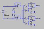
Attempting to fight the ESS hump. Yet another lost cause, I'm afraid, unless one decides to sacrifice some performances, to bury the hump in noise shit.I was wondering why you're using a 3rd order MFB after the DAC?
(well 4th if we take the I/V filter from the previous stage as well)
Bandwidth of ADC+DAC is about 200KHz, intended to cover 384KHz sampling (which currently doesn't work, appears to be an XMOS issue/bug with 32bit ADC input at high sample rates).What bandwith are you aiming for? It's now around 300kHz or so.
Doublecheck ANALYZER_ADC_IN.jpg, the input caps are there. Using non polarized electrolytics.Also there don't seem to be any input caps on the input section.
2.8k is low, but it's a compromise between using inverting configuration (to avoid common mode distortions) and bandwidth. Doesn't really matter, since there will be a high impedance analog front end, next step in this project.The input impedance is also rather low at 2k8 ohm?
I usually start with 0603 or 0805.
If the whole concept works, I will make it smaller if the design really needs it.
So do I, and now the proof of concept works, so it's time to make it smaller. I can now imagine a pocket size analog APx555
Last edited: