-
WANTED: Happy members who like to discuss audio and other topics related to our interest. Desire to learn and share knowledge of science required. There are many reviews of audio hardware and expert members to help answer your questions. Click here to have your audio equipment measured for free!
You are using an out of date browser. It may not display this or other websites correctly.
You should upgrade or use an alternative browser.
You should upgrade or use an alternative browser.
Audio analyzer project
- Thread starter syn08
- Start date
I believe that NXP has an open UAC2 implementation, but the uC officially supporting it cost even more than the XMOS ones.One thing that I was unable to make work is the ES9822 ADC @384KHz, with 49.152MHz MCLK. Everything is by the book (read: ESS datasheet), the ADC should work at 24.576MHz bit clock (and the MCLK divided by 2), 384KHz settings are by no means different than the settings for 96KHz and 192KHz (only different values), there's even a table in the data sheet with the registers settings for each mode (no need to put the ADC in 2x mode for 384KHz).
Doesn't work, the noise floor raises to absurd values (some -70dB). The DAC works beautiful at 384KHz... I gave up until a better (or luckier) detective than myself could identify a solution. This kind of detectivistic work is the only "secret sauce" of any ESS based implementation...
And a side note, as much as I hate the XMOS controllers (from almost every perspective, starting with the weird programming model, documentation that is everywhere and nowhere, licensing model, prices, and ending with the power intake) that's the only option for us mortals. Any other UAC2 solution is a best kept secret, I could rather get some information from the Pentagon than from those manufactures in Asia (CMedia, ComTrue, etc...) while a reliable and complete open source solution on a generic controller like the STMs doesn't really exist, and won't, since UAC3 is around the corner, eliminating most of the UAC2 mess (that is, the interface polling mechanism).
syn08
Senior Member
- Thread Starter
- #23
I believe that NXP has an open UAC2 implementation, but the uC officially supporting it cost even more than the XMOS ones.
Thanks, I've seen that, however the obvious target for the NXP SDK (i.MX RT600 Crossover MCUs) comes only in the DIY impossible 0.3-0.4mm pitch BGAs. I don't have the tooling to solder such chips (and not planning to invest in).
Barring some licensing fine print, the NXP source code could be a good starting point for developing an open source, portable, UAC2 stack. As I said, nobody seems to have the appettite for such, at least because UAC3 is around the corner.
syn08
Senior Member
- Thread Starter
- #24
It took another PCB iteration, to correct a few things:
- I wrongly placed my bet on the THS4551 differential amplifier for the ADC input; this otherwise excellent chip doesn't take well low loads, and the ES9822 ADC has only some 430 ohm input impedance. The THS4551 was replaced with standard OPA1612 dual op amps, much more tolerant to low loads.
- Some layout changes to improve the I/O balanced symmetry (affecting the 2nd harmonic results).
Still no THD compensations is used, and I concluded once again that the whole compensation is pretty much an useless feature. Let's start with this one:
- After much experimenting, I concluded that the THD compensation, both in the DAC and ADC have nothing to do with the ESS chips process variations; it only compensated for the external circuitry distortions (2nd and 3rd harmonics). What I have noticed while measuring the ADC/DAC analog loop is that I can compensate the ADC distortions by trimming the DAC compensation, and the other way around! This means that any method we would use for compensate for the ADC and DAC distortions would end up with a compromise.
Here are the final REW distortions measurements.
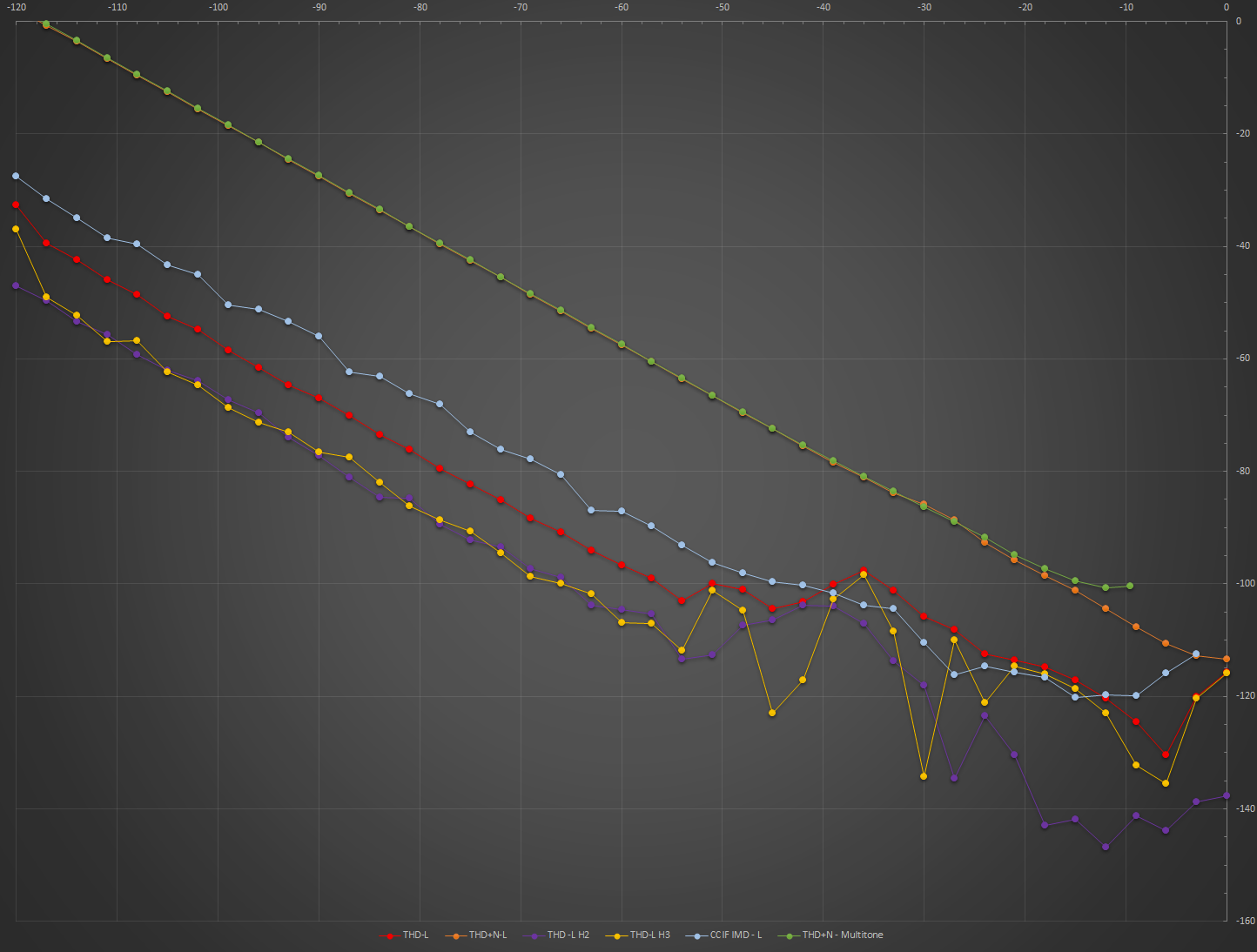
These are the analog loop distortions vs. Level measurements. Input frequency was 1KHz and sampling rate 48KHz, except for the CCIF IMD where it was 96KHz. Always recall that no DAC/ADC THD correction was used.
Comments:
- THD+N/SINAD (orange) reaches abut -115dB, and it is clearly noise limited (see the delta between the THD+N and the THD (red)) except close to 0dbFS where the 3rd harmonic (yellow) appears to dominate. This is not unexpected (0dBFS is 4.1Veff). Given there are two uncorrelated noise contributors (the DAC and the ADC) I believe 115dB SINAD is an excellent value. I have the feeling that the ADC is the major noise contributor, but I have no measurements to support this assumption.
- ESS hump. Once again, I concluded that the DAC ESS hump is impossible to avoid completely; all we can do is to minimize it's effect (by offsetting the I/V stage common mode bias, I used an 1V common mode bias). The strategy to lower the I/V stage gain is effective only because it affects the DAC SNR, therefore partially hiding the "hump" in noise. As you can see, all the THD measurements (THD (red), 2nd Harmonic (violet), 3rd Harmonic (yellow) and IMD (light blue)) appear to be affected by the "hump", and it is NOT the CCIF 19+20KHz IMD that is the most "hump" revealing measurement, since IMD values are also affected by noise, but the THD.
- The super symmetry of the I/O stages pays off; barring the hump effect, 2nd harmonics are down to around -140dB (take this number with a bit of salt, there's a rather large incertitude of measurements in this region). Even so, 2nd harmonic is much lower that the 3rd harmonic, which can be largely attributed to the op amp intrinsic and loading effect (3rd harmonic values are in the ballpark of the op amps data sheet specification).
- Barring the measurements incertitudes,the minimum THD is reached at about -6dBFS and is around -127dB, and the minimum IMD is around -10dBFS and reaches -120dB. I believe these results are very good.
- Finally, the multi tone THD+N follows almost perfectly the THD+N curve, up to about -20dBFS. However, the multi tone clipping level is, according to REW, at about -9dBFS, so this value must shift the multi tone THD+N curve to the right. One to another, I concluded that the THD+N and multi tone THD+N results are, for all practical purposes, identical.
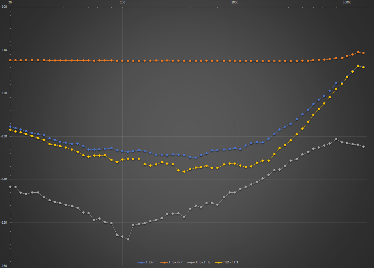
Here's the distortion vs. frequency measurement. Input signal was -9dBFS, from 20Hz to 30KHz, sampling was 192KHz.
Comments:
- As expected, the THD+N is rather flat, since noise dominates the measurements, except to beyond 20KHz, where the harmonics are taking over.
- Again as expected, the analog circuitry symmetrical layout and close tolerances pays off; the 2nd harmonic (grey) is much lower than the 3rd harmonic (yellow), even if we consider the large measurements uncertainty beyond -130dB. This is to say that the measured values in this range should be considered relative rather than absolute. Once again, the 3rd harmonic performance appears to be driven by the op amps; the values are more or less in line with their data sheets. I don't think there are better op amps today, matching all requirements (low distortions, large bandwidth, large current output) than the OPA1622 (DAC I/V stage) and the OPA1612 (ADC input stage).
- Regarding THD (blue) the magic threshold of -120dB is maintained at all frequencies under 20KHz. Make sure you recall that no THD correction "cheating" was used to get these results. With THD correction, I could get a commercially nice dip at 1KHz, while outside this frequency the THD would be larger, due to the asymmetries and poor tolerances. Or save money on parts, and promote the corrected THD dip values as the best thing since sliced bread .
.
The latest board version:
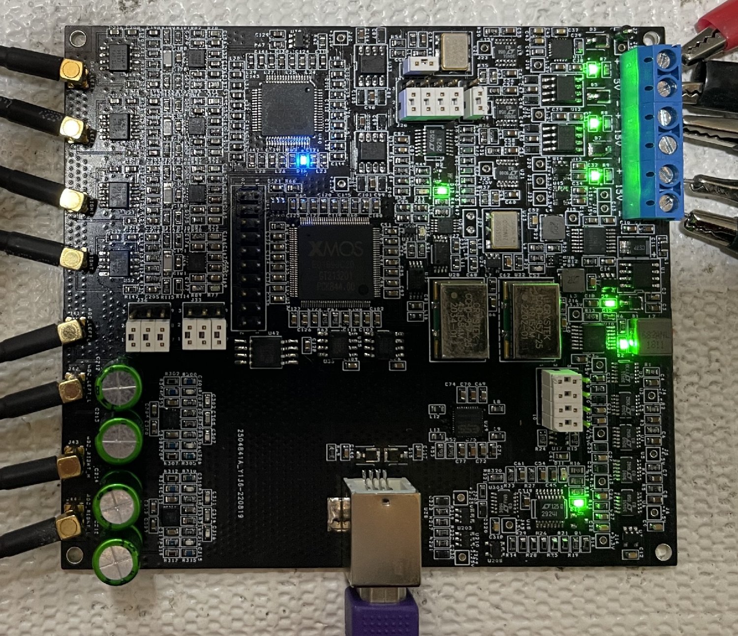
- I wrongly placed my bet on the THS4551 differential amplifier for the ADC input; this otherwise excellent chip doesn't take well low loads, and the ES9822 ADC has only some 430 ohm input impedance. The THS4551 was replaced with standard OPA1612 dual op amps, much more tolerant to low loads.
- Some layout changes to improve the I/O balanced symmetry (affecting the 2nd harmonic results).
Still no THD compensations is used, and I concluded once again that the whole compensation is pretty much an useless feature. Let's start with this one:
- After much experimenting, I concluded that the THD compensation, both in the DAC and ADC have nothing to do with the ESS chips process variations; it only compensated for the external circuitry distortions (2nd and 3rd harmonics). What I have noticed while measuring the ADC/DAC analog loop is that I can compensate the ADC distortions by trimming the DAC compensation, and the other way around! This means that any method we would use for compensate for the ADC and DAC distortions would end up with a compromise.
- Assume we have an ideal sine source with zero distortions and an ideal analyzer with zero residual distortions, and we trim the ADC and DAC THD using these; after the trimming, if we switch to the ADC/DAC analog loop, the results will be much worse than the sum of the trimmed distortions.
- If we trim the ADC and DAC using the analog loop (difficult, since we have two independent variables), then when inserting a DUT in the analog loop the analyzer residual distortions will be larger and essentially unknown.
- This explains why other builders are maintaining that using low tolerance components in the ADC input is not that important; of course it appears so, if you are using the ADC THD compensation to band aid this. The situation is conceptually the same as using a poor open loop amplifier and relying on negative feedback to fix it.
Here are the final REW distortions measurements.
These are the analog loop distortions vs. Level measurements. Input frequency was 1KHz and sampling rate 48KHz, except for the CCIF IMD where it was 96KHz. Always recall that no DAC/ADC THD correction was used.
Comments:
- THD+N/SINAD (orange) reaches abut -115dB, and it is clearly noise limited (see the delta between the THD+N and the THD (red)) except close to 0dbFS where the 3rd harmonic (yellow) appears to dominate. This is not unexpected (0dBFS is 4.1Veff). Given there are two uncorrelated noise contributors (the DAC and the ADC) I believe 115dB SINAD is an excellent value. I have the feeling that the ADC is the major noise contributor, but I have no measurements to support this assumption.
- ESS hump. Once again, I concluded that the DAC ESS hump is impossible to avoid completely; all we can do is to minimize it's effect (by offsetting the I/V stage common mode bias, I used an 1V common mode bias). The strategy to lower the I/V stage gain is effective only because it affects the DAC SNR, therefore partially hiding the "hump" in noise. As you can see, all the THD measurements (THD (red), 2nd Harmonic (violet), 3rd Harmonic (yellow) and IMD (light blue)) appear to be affected by the "hump", and it is NOT the CCIF 19+20KHz IMD that is the most "hump" revealing measurement, since IMD values are also affected by noise, but the THD.
- The super symmetry of the I/O stages pays off; barring the hump effect, 2nd harmonics are down to around -140dB (take this number with a bit of salt, there's a rather large incertitude of measurements in this region). Even so, 2nd harmonic is much lower that the 3rd harmonic, which can be largely attributed to the op amp intrinsic and loading effect (3rd harmonic values are in the ballpark of the op amps data sheet specification).
- Barring the measurements incertitudes,the minimum THD is reached at about -6dBFS and is around -127dB, and the minimum IMD is around -10dBFS and reaches -120dB. I believe these results are very good.
- Finally, the multi tone THD+N follows almost perfectly the THD+N curve, up to about -20dBFS. However, the multi tone clipping level is, according to REW, at about -9dBFS, so this value must shift the multi tone THD+N curve to the right. One to another, I concluded that the THD+N and multi tone THD+N results are, for all practical purposes, identical.
Here's the distortion vs. frequency measurement. Input signal was -9dBFS, from 20Hz to 30KHz, sampling was 192KHz.
Comments:
- As expected, the THD+N is rather flat, since noise dominates the measurements, except to beyond 20KHz, where the harmonics are taking over.
- Again as expected, the analog circuitry symmetrical layout and close tolerances pays off; the 2nd harmonic (grey) is much lower than the 3rd harmonic (yellow), even if we consider the large measurements uncertainty beyond -130dB. This is to say that the measured values in this range should be considered relative rather than absolute. Once again, the 3rd harmonic performance appears to be driven by the op amps; the values are more or less in line with their data sheets. I don't think there are better op amps today, matching all requirements (low distortions, large bandwidth, large current output) than the OPA1622 (DAC I/V stage) and the OPA1612 (ADC input stage).
- Regarding THD (blue) the magic threshold of -120dB is maintained at all frequencies under 20KHz. Make sure you recall that no THD correction "cheating" was used to get these results. With THD correction, I could get a commercially nice dip at 1KHz, while outside this frequency the THD would be larger, due to the asymmetries and poor tolerances. Or save money on parts, and promote the corrected THD dip values as the best thing since sliced bread
The latest board version:
Last edited:
Stinius
Member
- Joined
- Jan 14, 2022
- Messages
- 25
- Likes
- 23
I could have given your post a "Like", but I will give it more than a "Like" It is a very good post and impressive results, a comment on the last paragraph. "You are so right"It took another PCB iteration, to correct a few things:
- I wrongly placed my bet on the THS4551 differential amplifier for the ADC input; this otherwise excellent chip doesn't take well low loads, and the ES9822 ADC has only some 430 ohm input impedance. The THS4551 was replaced with standard OPA1612 dual op amps, much more tolerant to low loads.
- Some layout changes to improve the I/O balanced symmetry (affecting the 2nd harmonic results).
Still no THD compensations is used, and I concluded once again that the whole compensation is pretty much an useless feature. Let's start with this one:
- After much experimenting, I concluded that the THD compensation, both in the DAC and ADC have nothing to do with the ESS chips process variations; it only compensated for the external circuitry distortions (2nd and 3rd harmonics). What I have noticed while measuring the ADC/DAC analog loop is that I can compensate the ADC distortions by trimming the DAC compensation, and the other way around! This means that any method we would use for compensate for the ADC and DAC distortions would end up with a compromise.
- Anyways, I concluded that it is much more reasonable to keep these corrections at zero, and optimize the analog I/O stages for minimum distortions (so almost nothing has to be corrected). These optimizations include choosing the best op amps (here, OPA1622 for the DAC IV stage and OPA1612 for the ADC input stage), optimizing the layout for super symmetry and using 0.1% or better components to preserve the symmetry (minimizing the 2nd harmonics). As a plus, such optimizations are largely frequency and level independent, which the THD corrections are not.
- Assume we have an ideal sine source with zero distortions and an ideal analyzer with zero residual distortions, and we trim the ADC and DAC THD using these; after the trimming, if we switch to the ADC/DAC analog loop, the results will be much worse than the sum of the trimmed distortions.
- If we trim the ADC and DAC using the analog loop (difficult, since we have two independent variables), then when inserting a DUT in the analog loop the analyzer residual distortions will be larger and essentially unknown.
- This explains why other builders are maintaining that using low tolerance components in the ADC input is not that important; of course it appears so, if you are using the ADC THD compensation to band aid this. The situation is conceptually the same as using a poor open loop amplifier and relying on negative feedback to fix it.
Here are the final REW distortions measurements.
These are the analog loop distortions vs. Level measurements. Input frequency was 1KHz and sampling rate 48KHz. Always recall that no DAC/ADC THD correction was used.
View attachment 228908
Comments:
- THD+N/SINAD (orange) reaches abut -115dB, and it is clearly noise limited (see the delta between the THD+N and the THD (red)) except close to 0dbFS where the 3rd harmonic (yellow) appears to dominate. This is not unexpected (0dBFS is 4.1Veff). Given there are two uncorrelated noise contributors (the DAC and the ADC) I believe 115dB SINAD is an excellent value. I have the feeling that the ADC is the major noise contributor, but I have no measurements to support this assumption.
- ESS hump. Once again, I concluded that the DAC ESS hump is impossible to avoid completely; all we can do is to minimize it's effect (by offsetting the I/V stage common mode bias, I used an 1V common mode bias). The strategy to lower the I/V stage gain is effective only because it affects the DAC SNR, therefore partially hiding the "hump" in noise. As you can see, all the THD measurements (THD (red), 2nd Harmonic (violet), 3rd Harmonic (yellow) and IMD (light blue)) appear to be affected by the "hump", and it is NOT the CCIF 19+20KHz IMD that is the most "hump" revealing measurement, since IMD values are also affected by noise, but the THD.
- The super symmetry of the I/O stages pays off; barring the hump effect, 2nd harmonics are down to around -140dB (take this number with a bit of salt, there's a rather large incertitude of measurements in this region). Even so, 2nd harmonic is much lower that the 3rd harmonic, which cab be largely attributed to the op amp intrinsic and loading effect (3rd harmonic values are in the ballpark of the op amps data sheet specification).
- Barring the measurements incertitudes,the minimum THD is reached at about -6dBFS and is around -127dB, and the minimum IMD is around -10dBFS and reaches -120dB. I believe these results are very good.
- Finally, the multi tone THD+N follows almost perfectly the THD+N curve, up to about -20dBFS. However, the multi tone clipping level is, according to REW, at about -9dBFS, so this value must shift the multi tone THD+N curve to the right. One to another, I concluded that the THD+N and multi tone THD+N results are, for all practical purposes, identical.
Here's the distortion vs. frequency measurement. Input signal was -9dBFS, from 20Hz to 30KHz, sampling was 192KHz.
View attachment 228913
Comments:
- As expected, the THD+N is rather flat, since noise dominates the measurements, except to beyond 20KHz, where the harmonics are taking over.
- Again as expected, the analog circuitry symmetrical layout and close tolerances pays off; the 2nd harmonic (grey) is much lower than the 3rd harmonic (yellow), even if we consider the large measurements uncertainty beyond -130dB. This is to say that the measured values in this range should be considered relative rather than absolute. Once again, the 3rd harmonic performance appears to be driven by the op amps; the values are more or less in line with their data sheets. I don't think there are better op amps today, matching all requirements (low distortions, large bandwidth, large current output) than the OPA1622 (DAC I/V stage) and the OPA1612 (ADC input stage).
- Regarding THD (blue) the magic threshold of -120dB is maintained at all frequencies under 20KHz. Make sure you recall that no THD correction "cheating" was used to get these results. With THD correction, I could get a commercially nice dip at 1KHz, while outside this frequency the THD would be larger, due to the asymmetries and poor tolerances. Or save money on parts, and promote the corrected THD dip values as the best thing since sliced bread.
Stein
syn08
Senior Member
- Thread Starter
- #26
A note on the ESS chips.
While I never had any issues with the ESS Dac chips (other than the ubiquitous "hump"), the other ESS chips I experimented with had some serious problems:
- ES9311 (low noise power supply, Imax=150mA) has some serious reliability issues. I've destroyed about 20 chips while experimenting, they simply die at power on (or power off) without exceeding any spec in the data sheet. Never seen such before with a linear chip, and I am 100% sure no voltage spikes were involved in the crashes. The only correlation I was able to identify is with the noise filtering capacitors, anything over 10uF (either ceramic or tantalum polymer) almost guarantee, sooner or later, the chip destruction. I completely gave up using these chips, they are cheap compared to other very low noise regulators (LT3045, ADM7154) but way to fragile, unless somebody specifies further maximum ratings in the datasheet. Don't expect this IC to be your next low cost plug and play low noise regulator.
ES9822 ADC. Others identified a performance fluctuation from chip to chip. I can confirm these fluctuations, not so much in the THD performance (without THD correction), but in the SINAD performance. I have noted +/-4-5dB variations from chip to chip, usually observed as an unexplained rise (up to 6-10dB) of noise and spurious toward high frequencies at 192KHz sample rate. Strange, since this ADC chip doesn't seem to implement any noise shaping strategy, some chips are ruler flat. Also, these chips appear to be quite fragile, I had a few experiencing weird failures, from occasionally failing to switch the sampling frequency (via software/registers), to I2C bus failures, to very high noise (some -100dB compared to the usual about -160dB @48KHz and 1M samples). Nowhere close to the failure rates of the ES9311, but still indicating some lack of integration with the silicon foundry processes variations?
Well, the ESS chips are addressing a niche market anyway, so I am not holding my breath for ESS to re-design any of these to make them more robust. Perhaps the next generation chips will show some "lessons learned".
Here's an example of a noisy ES9822. THD @192KHz sampling is ok, but THD+N is 8-10dB worse compared to a top performer (-104dB, at this sampling rate). Same DAC, of course.
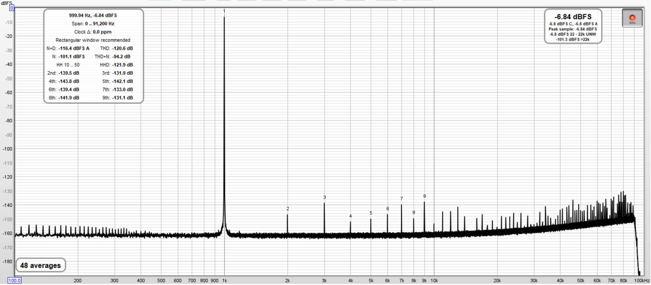
The RMS quantization noise level is about -105dB (-162dB FFT noise floor + 57dB process gain (1M FFT points)) which would be fine @192KHz sampling rate. Add 6dB to the above numbers to calculate the FS SNR, since the signal is -6dB.
To show this is strictly a high frequency noise problem, at 48KHz sampling rate:
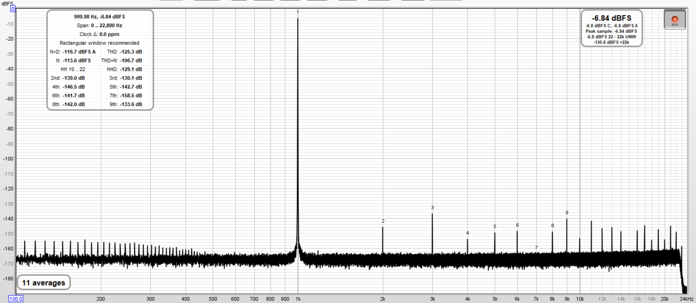
THD and THD+N are as good as one can get, without the distortion compensation cheating. The RMS quantization noise level is -107dB, for a calculated SNR of -113dB at FS. Assuming equal noise contributions from the DAC and ADC, this would lead to a SNR of -117dB for each (19.1 bit ENOB) which is IMO as good as one can get today from a delta-sigma 24bit ADC or DAC.
While I never had any issues with the ESS Dac chips (other than the ubiquitous "hump"), the other ESS chips I experimented with had some serious problems:
- ES9311 (low noise power supply, Imax=150mA) has some serious reliability issues. I've destroyed about 20 chips while experimenting, they simply die at power on (or power off) without exceeding any spec in the data sheet. Never seen such before with a linear chip, and I am 100% sure no voltage spikes were involved in the crashes. The only correlation I was able to identify is with the noise filtering capacitors, anything over 10uF (either ceramic or tantalum polymer) almost guarantee, sooner or later, the chip destruction. I completely gave up using these chips, they are cheap compared to other very low noise regulators (LT3045, ADM7154) but way to fragile, unless somebody specifies further maximum ratings in the datasheet. Don't expect this IC to be your next low cost plug and play low noise regulator.
ES9822 ADC. Others identified a performance fluctuation from chip to chip. I can confirm these fluctuations, not so much in the THD performance (without THD correction), but in the SINAD performance. I have noted +/-4-5dB variations from chip to chip, usually observed as an unexplained rise (up to 6-10dB) of noise and spurious toward high frequencies at 192KHz sample rate. Strange, since this ADC chip doesn't seem to implement any noise shaping strategy, some chips are ruler flat. Also, these chips appear to be quite fragile, I had a few experiencing weird failures, from occasionally failing to switch the sampling frequency (via software/registers), to I2C bus failures, to very high noise (some -100dB compared to the usual about -160dB @48KHz and 1M samples). Nowhere close to the failure rates of the ES9311, but still indicating some lack of integration with the silicon foundry processes variations?
Well, the ESS chips are addressing a niche market anyway, so I am not holding my breath for ESS to re-design any of these to make them more robust. Perhaps the next generation chips will show some "lessons learned".
Here's an example of a noisy ES9822. THD @192KHz sampling is ok, but THD+N is 8-10dB worse compared to a top performer (-104dB, at this sampling rate). Same DAC, of course.
The RMS quantization noise level is about -105dB (-162dB FFT noise floor + 57dB process gain (1M FFT points)) which would be fine @192KHz sampling rate. Add 6dB to the above numbers to calculate the FS SNR, since the signal is -6dB.
To show this is strictly a high frequency noise problem, at 48KHz sampling rate:
THD and THD+N are as good as one can get, without the distortion compensation cheating. The RMS quantization noise level is -107dB, for a calculated SNR of -113dB at FS. Assuming equal noise contributions from the DAC and ADC, this would lead to a SNR of -117dB for each (19.1 bit ENOB) which is IMO as good as one can get today from a delta-sigma 24bit ADC or DAC.
Last edited:
syn08
Senior Member
- Thread Starter
- #28
I am manually hot air soldering QFN/DFN chips for years now; after preparing the location, it takes me about 10-15 seconds (excluding pre-heating) for heating and get it soldered. I use exclusively leaded 63/37, don't even think of touching leadless alloys for such 0.4mm fine pitch devices as the ES9822.
While certainly not ideal, I have never seen any chips degrading performance or destroyed in the process.
While certainly not ideal, I have never seen any chips degrading performance or destroyed in the process.
Last edited:
Howdy, your regulator failures with low impedance ceramic caps could be input overshoot on turn on? the capacitor resonates with the circuit trace/leads causing the input voltage to spike. Easily fixed with series resistor, protective diodes won't be fast enough. Could also be stability issues if used on output (too low ESR).
syn08
Senior Member
- Thread Starter
- #30
Howdy, your regulator failures with low impedance ceramic caps could be input overshoot on turn on? the capacitor resonates with the circuit trace/leads causing the input voltage to spike. Easily fixed with series resistor, protective diodes won't be fast enough. Could also be stability issues if used on output (too low ESR).
Apparently there are already resistors in series with the recommended ceramic output cap, to tame the potential stability issues, since the output uF cap is connected to a device pin, and there's only a 100's of pF cap required directly at the regulator output.. But then anything is possible, and I am sure solutions could be developed, using all kind of tricks in the bag, including resistors in series, protection Schottky diodes, etc... My expectation was though to use the simple application illustrated in the data sheets. It is impossible to experiment much with these 0.4mm pitch QFN devices, and I am not about to do the ESS applications engineers work, for free, anyway. So they are out of my BOMs.
Last edited:
I meant also in series with the input supply but yes some chips are not worth bothering with. My personal favorite was a TI LVDS receiver with no ESD protection where they seemed to randomly fail in transit but never once installed, the mystery was solved when I found the 'reduced ESD protection' footnote.
syn08
Senior Member
- Thread Starter
- #32
I meant also in series with the input supply but yes some chips are not worth bothering with. My personal favorite was a TI LVDS receiver with no ESD protection where they seemed to randomly fail in transit but never once installed, the mystery was solved when I found the 'reduced ESD protection' footnote.
Well, good luck finding any relevant footnote about or, more general, any decent data sheet coming from ESS
BTW, according to my experience, the input cap does not have any effect on the failures. The problem appears to be related to the RFLT bandgap reference noise bypass capacitor (and the associated FLT1 and FLT2 caps). Increasing these caps over the apparently standard 1uF ceramic (to lower the LF noise, which is otherwise not that great) may lead to chip failures. In despite the fact that Fig. 9, Fig. 10 and Fig. 11 in the ES9311 data sheet clearly states that 10uF caps were used.
In general, up to 100KHz, noise is slightly worse compared to LT3045 or the ADM7154 and quite rising past 100KHz, and the HF PSRR is also not that great. That, without any incentives to design with this chip (other than the low price). The QFN 0.4mm pitch is also a PITA for those not willing to invest in reflow equipment, like myself.
Last edited:
syn08
Senior Member
- Thread Starter
- #33
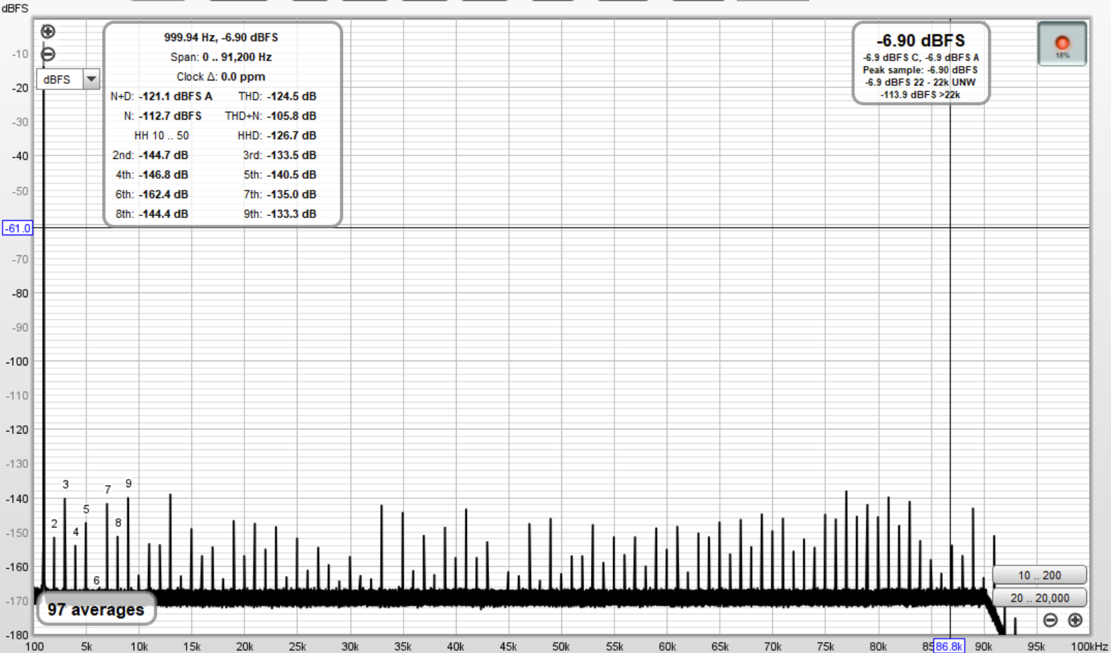
Example of ruler flat noise, noise floor @192KHz sampling rate is about the same as in post #26... Frequency scale is this time linear, to show that only harmonic components are generated (no spurious).
THD+N is 11dB better with this chip, which is HUGE, in my opinion. The noise floor is ruler flat, and THD is also slightly better. This chip meets or exceeds the data sheet spec (THD+N -113dB @192KHz -1dBFS), if you add 5dB to the signal and subtract 3dB from the noise, to account for the DAC noise. The chip in #26 does not (measures only -103dB THD+N, after signal/noise normalization). Both chips were tested on the same board, so no other variables are involved, except the ES9822 chip itself.
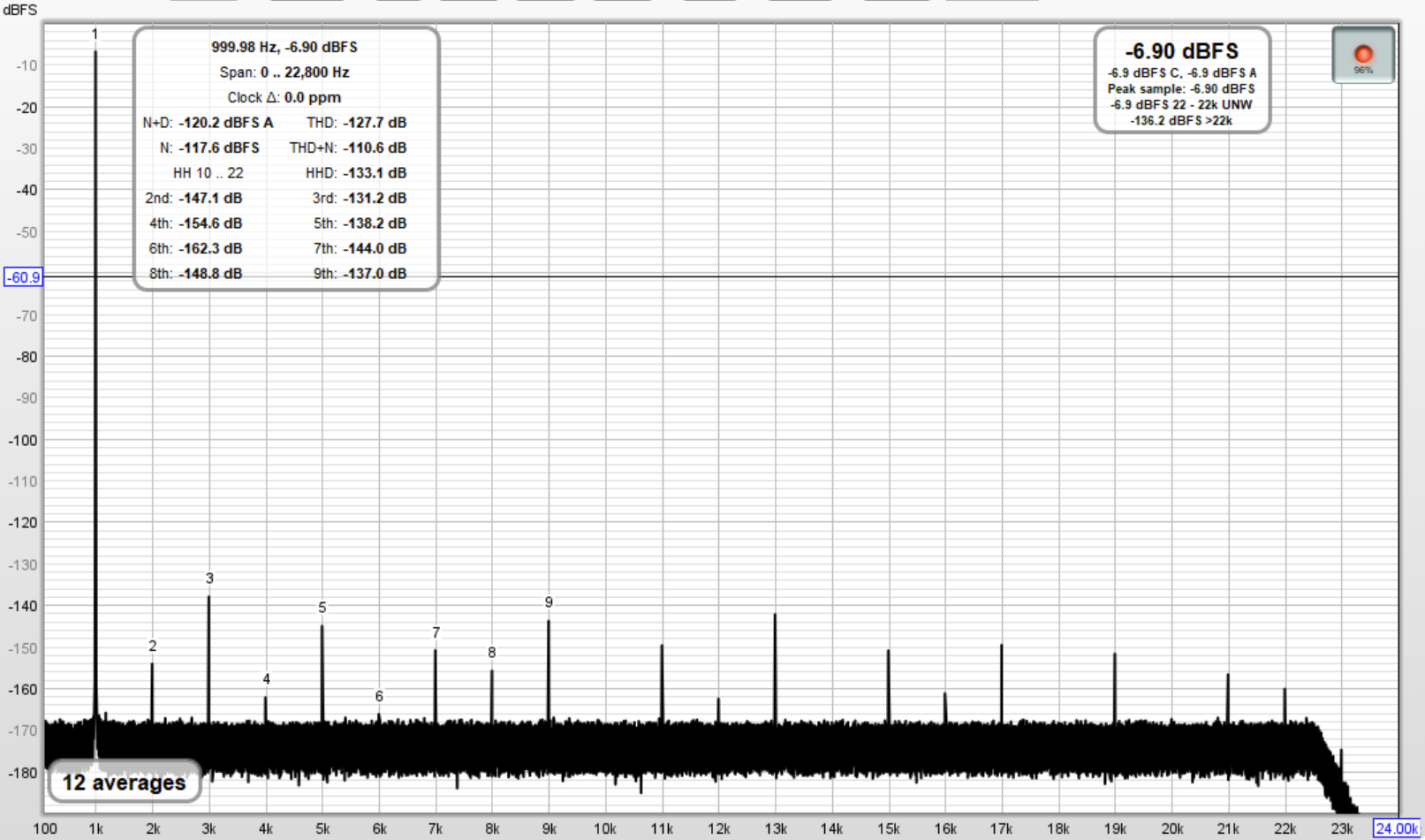
@48KHz sampling rate (everything else is unchanged), the same story; THD+N meets or slightly exceeds the data sheet spec of typical -117dB and max. -114dB (after S/N normalization). The chip in #26 fails short, with only -113dB, although the delta (1dB) is within the measurement uncertainty. This shows once again that the performance problem is at high frequencies. Meaning that characterizing the performance at 1KHz only, using the THD compensation "cheat", and a tuned notch filter in the front end, is incomplete for instrumentation purposes, unless the end user plans to use the ADC at 1KHz (or other fixed frequency) only...
BTW, all measurements above are in stereo mode.
THD+N is 11dB better with this chip, which is HUGE, in my opinion. The noise floor is ruler flat, and THD is also slightly better. This chip meets or exceeds the data sheet spec (THD+N -113dB @192KHz -1dBFS), if you add 5dB to the signal and subtract 3dB from the noise, to account for the DAC noise. The chip in #26 does not (measures only -103dB THD+N, after signal/noise normalization). Both chips were tested on the same board, so no other variables are involved, except the ES9822 chip itself.
@48KHz sampling rate (everything else is unchanged), the same story; THD+N meets or slightly exceeds the data sheet spec of typical -117dB and max. -114dB (after S/N normalization). The chip in #26 fails short, with only -113dB, although the delta (1dB) is within the measurement uncertainty. This shows once again that the performance problem is at high frequencies. Meaning that characterizing the performance at 1KHz only, using the THD compensation "cheat", and a tuned notch filter in the front end, is incomplete for instrumentation purposes, unless the end user plans to use the ADC at 1KHz (or other fixed frequency) only...
BTW, all measurements above are in stereo mode.
Last edited:
OWC
Active Member
- Joined
- Apr 14, 2019
- Messages
- 204
- Likes
- 154
It's a little hard to follow, but are those numbers with or without the input section?
Or is it just direct in - direct out?
It's a little hard to judge what exactly is going on without a schematic/PCB.
I had the occasional ADC/DAC in the past that was very picky for board layout, or the right decoupling.
I also had some issues with a weird oscillation in an ADC once, because of some odd power-on sequence.
syn08
Senior Member
- Thread Starter
- #36
Schematics attached. There could be a few values that need to be updated, though... As I said, there's nothing outstanding (essentially datasheet applications for the ADC/DAC and the core from the XMOS audio demo board), other than likely over engineered power supplies (note the rigorous power sequencing for each subsystem) and the presence of two items that are not really required (can be omitted from soldering): the DAC programmable clock (I wanted to estimate the delta between synchronous and asynchronous DAC/ADC operation) and the clocking programmable PLL (intended to replace the expensive Crystek clocks). Some of the large caps used for decoupling (in particular for high impedance points, like the reference voltages) are actually tantalum polymer rather than X7R ceramics, the schematics are not showing them as polarized caps. X7R ceramics are used in all low impedance points decoupling.
Gerbers to follow ASAP.
Gerbers to follow ASAP.
Attachments
syn08
Senior Member
- Thread Starter
- #37
Gerbers (exactly as sent to JLCPCB) attached. Friendly warning: if you don't have the proper tools and a technician to do the assembly/rework for you (or if you don't have good technician skills like myself  ) don't even think about attempting to solder this rather dense 4 layers board. You may easily end up with an expensive pile of junk silicon. Can somebody imagine the size of a board with through hole components
  ?
?
I'm planning an even more dense board, with 0402 parts (this is with 0603) and without the configuration pins (which were useful during development and testing). This will be probably 2/3 the area of the current board.
I'm planning an even more dense board, with 0402 parts (this is with 0603) and without the configuration pins (which were useful during development and testing). This will be probably 2/3 the area of the current board.
Attachments
OWC
Active Member
- Joined
- Apr 14, 2019
- Messages
- 204
- Likes
- 154
For prototyping, I stopped using 0402.Gerbers (exactly as sent to JLCPCB) attached. Friendly warning: if you don't have the proper tools and a technician to do the assembly/rework for you (or if you don't have good technician skills like myself) don't even think about attempting to solder this rather dense 4 layers board. You may easily end up with an expensive pile of junk silicon. Can somebody imagine the size of a board with through hole components
?
I'm planning an even more dense board, with 0402 parts (this is with 0603) and without the configuration pins (which were useful during development and testing). This will be probably 2/3 the area of the current board.
Yes it's doable and I can solder it without problems, but it's not worth all the extra hassle.
I usually start with 0603 or 0805.
If the whole concept works, I will make it smaller if the design really needs it.
OWC
Active Member
- Joined
- Apr 14, 2019
- Messages
- 204
- Likes
- 154
Nothing major I see, except for just a few different things, but that is a matter of taste. 
I was wondering why you're using a 3rd order MFB after the DAC?
(well 4th if we take the I/V filter from the previous stage as well)
What bandwith are you aiming for? It's now around 300kHz or so.
Also there don't seem to be any input caps on the input section.
The input impedance is also rather low at 2k8 ohm?
Last edited:
Similar threads
- Replies
- 26
- Views
- 2K
- Replies
- 9
- Views
- 3K
