• WANTED: Happy members who like to discuss audio and other topics related to our interest. Desire to learn and share knowledge of science required. There are many reviews of audio hardware and expert members to help answer your questions. Click here to have your audio equipment measured for free!

Simulation of Crossover Distortions and design Class-AB with THD=0.00002% / 100W / 20kHz

  • Thread starter Deleted member 27948
  • Start date
D

Deleted member 27948

Guest
Dear Audio Scientists,

Recently I had fun simulating crossover distortions in Class-AB amplifiers with nested feedback loops.

It was quite interesting and I would like to share the results of my study:
1) It's a bit more productive to look at feedback as means to take a derivative of distortions rather than a plain attenuator of distortions.
2) Being a differentiator, feedback "shifts" non-linear distortions to high frequencies
3) Feedback can be nested, with each loop shifting the distortions up and up.
4) By itself, no amount of fedback can eliminate distortions, but their high-frequency remnants can be filtered with a passive LC filter, same as in class-D.
5) The end distortions are inversely proportional to Iq and Gain Bandwidth Product of amplifier, for nested feedback GBP^n

An example of such design loosely based on "blameless" amplifier by D. Self, with two 2nd-order feedback loops:

1619848399530.png


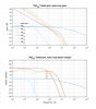
Here are the distortions of the "blameless" amplifier itself, for Iq=20mA, 20kHz 100W. Only the envelope of harmonics is plotted in frequency domain, not the mess between harmonics because that mess is due to calculation errors and has nothing to do with reality.
1619848877994.png

and here are the distortions for the entire design:
1619849145185.png


A full description of the MATLAB package with LTspice schematics can be found at: https://www.mathworks.com/matlabcen...crossover-distortions-in-class-ab-0-00002-thd

As with any simulations untested in the real-life, you can never be 100% sure that it's all true but... please let me know how and where I screwed up.
 

pma

Major Contributor
Joined
Feb 23, 2019
Messages
4,602
Likes
10,771
Location
Prague
Hi @mt42 and welcome in the forum!
Nice simulation and results look good. With a low distortion circuit like this, PCB design and power supply and signal wiring may and probably will say the last word in the real world distortion and S/N obtained. Looking forward to see your functional sample results!
 

pma

Major Contributor
Joined
Feb 23, 2019
Messages
4,602
Likes
10,771
Location
Prague
BTW, C8 = 723nF and R2 = 2k2 make input high pass filter with a cut off frequency (100Hz) too high for audio, this should be corrected.

The same for R4, C3. C3 should be at least 100 uF. Would you kindly post simulated FR and loopgain?
 
Last edited:
OP
D

Deleted member 27948

Guest
Correct. the nominal of 723nF was used to "show" that it's not a real value. C3R4 ~1kHz. You can't use real Cx values for LTspice simulations because low-frequency transient processes would take "forever" - but we are no interested in them. Even with such high values, it takes minutes on i7.

Good question on loop gain, which are a few.
1619898577478.png

Ab0 - just output stage
AB1 - blameless amp with 1st order loopback
AB2 - " - 2nd order
AB3 - add op-amp with 1st order loopback
AB4 - " - 2nd order
AB5 - add passive LC on the output.

I tried to attach .pdf with all the details, the same as on matlab site, but I got a msg that it's too large.
 

Attachments

  • 1619898500946.png
    1619898500946.png
    169.3 KB · Views: 100

pma

Major Contributor
Joined
Feb 23, 2019
Messages
4,602
Likes
10,771
Location
Prague
V6 is to simulate loopgain, right? The plots you posted are open loop gain, am I wrong? The compensation is TMC?
 
OP
D

Deleted member 27948

Guest
1) right. 2) no, you are not wrong. 3) I do not know what TMC is. It's a second-order astatism loop in automatic control theory jargon.
 
OP
D

Deleted member 27948

Guest
yes, TMC is pretty much equal to the old-fashioned 2nd-degree loopback. It's not clear why to invent a new name for it. Moreover, it's not necessarily Miller. The 2-nd order feedback works the same for a single-stage pseudo - cascode.

1619934078550.png


Yes, I know, the real-world is great, I know. That's why I stated explicitly that its' only simulation.

I am waiting for the decision of a good friend of mine who is a principal RF EE. Without him, it will take me way too long to do all the mistakes and learn from them.
 

AnalogSteph

Major Contributor
Joined
Nov 6, 2018
Messages
3,391
Likes
3,339
Location
.de
Be warned that SPICE simulation of BJT Ccb modulation tends to not be accurate enough to predict nonlinear distortion generated by it (particularly an issue in input LTP). As a rule of thumb, results with BJTs are too optimistic, while MOSFETs tend to be too pessimistic.

Also, the layout is going to be very, very important if real-life performance is supposed to be even close to simulation. Rail-to-rail and rail-to-ground inductance must be kept low, for example.
http://www.douglas-self.com/ampins/dipa/dipa.htm
https://neurochrome.com/pages/taming-the-lm3886-chip-amplifier
 
OP
D

Deleted member 27948

Guest
Be warned that SPICE simulation of BJT Ccb modulation tends to not be accurate enough to predict nonlinear distortion generated by it (particularly an issue in input LTP). As a rule of thumb, results with BJTs are too optimistic, while MOSFETs tend to be too pessimistic.

Also, the layout is going to be very, very important if real-life performance is supposed to be even close to simulation. Rail-to-rail and rail-to-ground inductance must be kept low, for example.
http://www.douglas-self.com/ampins/dipa/dipa.htm
https://neurochrome.com/pages/taming-the-lm3886-chip-amplifier

Well... As a retired mathematician, I do not understand how "normal" EE could use LTspice _properly_. Even for me, it was not easy to set everything up so that it gives physically meaningful and robust results.

I more than agree with you about layout. I can not find anyone who would take on this task. My friends, all being principal EE, admitted the insufficient experience and declined.

Do you know anyone who would want to be a partner in such a project?
 

H-713

Senior Member
Joined
Jan 24, 2021
Messages
379
Likes
666
I can tell you that the physical layout (and grounding!!!) nonidealities often dominate the distortion of most power amplifiers. Even getting something down in the 0.005% range is far from trivial in this regard. Getting below 0.0005% is going to be extremely difficult. You'll also need an audio analyzer than can reliably measure distortion that low. That isn't cheap. You'll need a big dummy load with an extremely low voltage coefficient of resistance as well.

Also, a single pair of 2SA1943 / 2SC5200 output devices is pretty borderline for a 100W power amplifier.
 

peufeu

Member
Joined
May 8, 2021
Messages
17
Likes
16
This is a neat design. I'm interested in nested feedback amps, so I like it. A few remarks:

The bottom pin of C11 is usually connected to the output of the amp, I wonder why it is connected to GND.

Do not trust Spice opamp models for distortion. Most cheat and do not model the internal circuitry, it's just a bunch of controlled current/voltage sources so you get correct frequency response. Usually the output stage is modelled, with transistor models of dubious quality. But the internal distortion is often not modelled at all.

I have doubts about the safe operating area of the drivers and the outputs, and big doubts about the current capability of the drivers. especially at high output current when the output transistor hFe drops.

0.1R emitter resistors may be too low to prevent thermal runaway, that depends on the thermal interface material between the transistors and the heatsink. Thermal runaway math is pretty simple, if the transistor heats by 1°C, Vbe decreases by dVbe=-2mV, so Ie increases by di=-dVbe/Re=20mA, so dissipated power increases by dP=Vce*di=0.67W, so temperature increases by dT=dP*RthJS. For stability you want each dT to cause a smaller dT with some margin, otherwise it'll run away. The Vbe multiplier bias transistor will compensate for the temperature of the heatsink, but not the temperature of the power transistor. So I'm considering the heatsink as isothermal and RthJS is the thermal resistance between the transistor and the heat sink. Here a good target would be RthJS=1°C/W or lower, there's 0.83°C/W in the device, that doesn't leave much for the thermal interface material. So you should test it from a bench power supply with current limit.

If you use 2 pairs of output transistors, with each at half the bias, same total dissipation, the magic of BJT transconductance means you can double your emitter resistors and you get the exact same crossover, but 2x less thermal runaway, and 2x more output current capability, with less hFe loss at high current, so less work for the drivers.

An interesting test to do is to set the input to 0V and inject a sine current into the output. You can then measure the crossover distortion, which only depends on output current and will be pretty much the same as when testing with an input signal and current in a resistive load, but without the signal getting in the way, so it is much more visible.

The open loop gain can vary with output current since output transistor fT is current dependent, also depends on Vce near saturation, so it is a good idea to plot open loop gain while stepping input voltage, around +/-1A output current, and also output near the rails. That way if there's a surprise burst of oscillation after clipping, you'll catch it.
 
OP
D

Deleted member 27948

Guest
I can tell you that the physical layout (and grounding!!!) nonidealities often dominate the distortion of most power amplifiers. Even getting something down in the 0.005% range is far from trivial in this regard. Getting below 0.0005% is going to be extremely difficult. You'll also need an audio analyzer than can reliably measure distortion that low. That isn't cheap. You'll need a big dummy load with an extremely low voltage coefficient of resistance as well.

Also, a single pair of 2SA1943 / 2SC5200 output devices is pretty borderline for a 100W power amplifier.

I absolutely agree. That's why simulation and implementation are different projects, with measurement algorithms being far from trivial. No, you can't use an audio analyzer. But... you can use an evaluation board for the latest and greatest TI's high-speed ADC - only $199 for the proven design and implementation. Then you collect lots of data in a special pulsed mode (not a constant level - it surely won't work), load it into MATLAB, and use full-power kernel adaptive methods to identify exactly what you need, together with reproducible confidence margins. Yet, I think you can't get below ADC analog input non-linearities no matter what, even if you put a null at fs.
 
Last edited by a moderator:
OP
D

Deleted member 27948

Guest
A. The bottom pin of C11 is usually connected to the output of the amp, I wonder why it is connected to GND.

B. I have doubts about the safe operating area of the drivers and the outputs, and big doubts about the current capability of the drivers. especially at high output current when the output transistor hFe drops. 0.1R emitter resistors may be too low to prevent thermal runaway, that depends on the thermal interface material...

C. An interesting test to do is to set the input to 0V and inject a sine current into the output. You can then measure the crossover distortion, which only depends on output current and will be pretty much the same as when testing with an input signal and current in a resistive load, but without the signal getting in the way, so it is much more visible.

D. The open loop gain can vary with output current since output transistor fT is current dependent, also depends on Vce near saturation, so it is a good idea to plot open loop gain while stepping input voltage, around +/-1A output current, and also output near the rails. That way if there's a surprise burst of oscillation after clipping, you'll catch it.

Thank you!

A. yes, I know and strongly disagree because that way you rely on implicit assumptions on how the output stage behaves above f-3. I analyzed it theoretically and modelled it. No good, amp becomes prone to ringing.

B. I am not planning to provide constant full power (which does not happen on music). Peak power of 100W, but long term thermal power ... 10W shall be plenty. I thought that the amplifier shall err on the safe side and have a small negative Iq / temp coefficient... what do I miss?

C. I am not sure I understood you. If I did, I don't see how the results will be interpretable for reactive loads because distortions happen at the current's zero-crossing. But yes, I agree, measurements will be very tricky.

D. Yes, that modelling has been done for both open-loop gain and distortions vs output bias in the range [-24... +24] V.
 

DonH56

Master Contributor
Technical Expert
Forum Donor
Joined
Mar 15, 2016
Messages
7,895
Likes
16,714
Location
Monument, CO
I absolutely agree. That's why simulation and implementation are different projects, with measurement algorithms being far from trivial. No, you can't use an audio analyzer. But... you can use an evaluation board for the latest and greatest TI's high-speed ADC - only $199 for the proven design and implementation. Then you collect lots of data in a special pulsed mode (not a constant level - it surely won't work), load it into MATLAB, and use full-power kernel adaptive methods to identify exactly what you need, together with reproducible confidence margins. Yet, I think you can't get below ADC analog input non-linearities no matter what, even if you put a null at fs.

I use Matlab, and various flavors of SPICE, but I do not know what the bold statements mean. But I am a lowly hairy-knuckled EE, not a scientist or mathematician, and have not used "full-power kernal adaptive methods" in design. I helped with VBIC (BJT/HBT SPICE) models to include quasi-sat and thermal effects but have mostly used Matlab for system-level analysis and test post-processing, not actual circuit analysis.

In general you won't get below the ADC's nonlinearities, but if you have reference source, you can measure and compensate for them to improve your measurement dynamic range. Fairly easy at DC, gets rapidly more difficult as you move up in frequency and as you perform dynamic (vs. steady-state sinusoidal) measurements. Note high-speed ADCs may not be the right choice for an audio measurement; higher-speed ADCs tend to have lower resolution, higher noise, and higher distortion than lower-frequency devices.
 

peufeu

Member
Joined
May 8, 2021
Messages
17
Likes
16
A. yes, I know and strongly disagree because that way you rely on implicit assumptions on how the output stage behaves above f-3. I analyzed it theoretically and modelled it. No good, amp becomes prone to ringing.

OK. I'm wondering about that too, so when the boards I ordered arrive I'll be sweeping a bunch of model output stages with the network analyzer, so I'll see what happens then. I'm quite curious to see if the models match.

> B. I am not planning to provide constant full power (which does not happen on music). Peak power of 100W, but long term thermal power

Well it's about the peaks, if you use 4 ohms speaker, and the "right" signal is played a bit loud, with 30V supplies you could get one 10A peak. 5 amps should happen a lot more often. Then with only one output device active, at this high current its hFe drops, so its base current increases quite dramatically, and the tiny driver transistor runs out of hFe too, so its base current increases, then both the predriver and the driver go into second breakdown and pop. This happens very quickly, it's not like slow overheating where you have time to turn it off.

It will also happen if the amp oscillates, which tends to occur when messing when the feedback to optimize it, in this case the cap between the driver emitters will save the output transistors by turning them off quickly and preventing cross-conduction. Without the cap, they won't turn off fast enough, so they'll both stay on, and there will be a loud bang as all the energy in the power supply caps is dumped into the output transistors. It's quite spectacular, I remember a chip amp that oscillated and the chip turned into a mini flamethrower.

You could use MJE15030/1/2 or D44H11/D45H11 as drivers, they're much beefier, and high fT to match your output transistors.

> C. I am not sure I understood you. If I did, I don't see how the results will be interpretable for reactive loads because distortions happen at the current's zero-crossing. But yes, I agree, measurements will be very tricky.

Yes, crossover distortion occurs at current zero crossing, and it'll be pretty much the same whatever the output voltage is, except near the rails where it gets worse. So you can measure it in isolation by setting the input voltage to zero, so the amp keeps its output voltage at zero too. Then, inject a current in the output, by replacing the load with a sine current source. The voltage that appears at the output depending on this current represents the output impedance of the amp, and it is nonlinear, that is the distortion that the amp would have added to a signal resulting in the same current. But there is no signal voltage, so it is a lot easier to measure. This ignores any distortion due to voltage, for example due to Cbc variations on the transistors.

> D. Yes, that modelling has been done for both open-loop gain and distortions vs output bias in the range [-24... +24] V.
 
  • Like
Reactions: 777
OP
D

Deleted member 27948

Guest
I use Matlab, and various flavors of SPICE, but I do not know what the bold statements mean. ... have mostly used Matlab for system-level analysis and test post-processing, not actual circuit analysis.

In general you won't get below the ADC's nonlinearities, but if you have reference source, you can measure and compensate for them to improve your measurement dynamic range. Fairly easy at DC, gets rapidly more difficult as you move up in frequency and as you perform dynamic (vs. steady-state sinusoidal) measurements. Note high-speed ADCs may not be the right choice for an audio measurement; higher-speed ADCs tend to have lower resolution, higher noise, and higher distortion than lower-frequency devices.

The best description of kernel methods "A shift in paradigm for system identification": https://www.tandfonline.com/doi/full/10.1080/00207179.2019.1578407
You can read mine https://www.mathworks.com/matlabcentral/fileexchange/83363-fast-subband-adaptive-filtering-fsaf but trust me Lennart Ljung's explanations are way more approachable.

MATLAB - LTspice interface, already referenced above: https://www.mathworks.com/matlabcen...crossover-distortions-in-class-ab-0-00002-thd

… provides low-level generic functionality such as
  • Read and write .sp / .net expanded netlist file
  • A component value get /set
  • An option get / set / delete
  • A command set / delete / modify
  • Process a netlist by LTspice: .OP, .AC or .TRAN
  • Read a variable (such as node voltage or current) or time / frequency
  • Bode plot for one or several variants
  • Plot THD in both time and frequency domains for one or several variants
  • Logging / self-test / utilities / etc
Class amp_ab.m
… provides higher-level functionality specific for Class AB audio amplifiers with a few assumptions, as R10 (8k…12k) is used to control Iq, certain node naming, etc:
  • Find out which values of R10 correspond to the chosen set of varying
    Iq = [5.0; 10.0; 20.0; 40.0; 80.0; 160.0] mA by inverse spline resampling.
  • Plot linearized ZIN for all stages of EF, various biases from Vee to Vcc and various Iq
  • Linearized Bode plot for chosen nodes and conditions
  • Plot detailed THD in time and frequency domains with intermediate results
  • Plot THD in time and frequency domains, including 3D mesh plots whenever appropriate for
  • A set of varying component values,
  • A set of varying Iq,
  • A set of varying amplitudes of input signal,
  • A set of varying frequencies of input signal
  • A set of different schematics.
Hope that helps.

Yes, I agree with your point about high-speed ADC. Alas, you need them because crossover distortions have a very wide spectrum, up to 10MHz. Also, you can get more resolution while downsampling manually ... but all that is pretty bad math.
 
OP
D

Deleted member 27948

Guest
Well it's about the peaks... It's quite spectacular, I remember a chip amp that oscillated and the chip turned into a mini flamethrower.

You could use MJE15030/1/2 or D44H11/D45H11 as drivers, they're much beefier, and high fT to match your output transistors.

Yes, crossover distortion occurs at current zero crossing, and it'll be pretty much the same whatever the output voltage is... But there is no signal voltage, so it is a lot easier to measure. This ignores any distortion due to voltage, for example due to Cbc variations on the transistors.

Thank you for so much info! Great to know.

Please let me contemplate your approach to measuring distortion. I need to translate your words into visualizations inside my poor old brain:)
 

DonH56

Master Contributor
Technical Expert
Forum Donor
Joined
Mar 15, 2016
Messages
7,895
Likes
16,714
Location
Monument, CO
The best description of kernel methods "A shift in paradigm for system identification": https://www.tandfonline.com/doi/full/10.1080/00207179.2019.1578407
You can read mine https://www.mathworks.com/matlabcentral/fileexchange/83363-fast-subband-adaptive-filtering-fsaf but trust me Lennart Ljung's explanations are way more approachable.

MATLAB - LTspice interface, already referenced above: https://www.mathworks.com/matlabcen...crossover-distortions-in-class-ab-0-00002-thd

… provides low-level generic functionality such as
  • Read and write .sp / .net expanded netlist file
  • A component value get /set
  • An option get / set / delete
  • A command set / delete / modify
  • Process a netlist by LTspice: .OP, .AC or .TRAN
  • Read a variable (such as node voltage or current) or time / frequency
  • Bode plot for one or several variants
  • Plot THD in both time and frequency domains for one or several variants
  • Logging / self-test / utilities / etc
Class amp_ab.m
… provides higher-level functionality specific for Class AB audio amplifiers with a few assumptions, as R10 (8k…12k) is used to control Iq, certain node naming, etc:
  • Find out which values of R10 correspond to the chosen set of varying
    Iq = [5.0; 10.0; 20.0; 40.0; 80.0; 160.0] mA by inverse spline resampling.
  • Plot linearized ZIN for all stages of EF, various biases from Vee to Vcc and various Iq
  • Linearized Bode plot for chosen nodes and conditions
  • Plot detailed THD in time and frequency domains with intermediate results
  • Plot THD in time and frequency domains, including 3D mesh plots whenever appropriate for
  • A set of varying component values,
  • A set of varying Iq,
  • A set of varying amplitudes of input signal,
  • A set of varying frequencies of input signal
  • A set of different schematics.
Hope that helps.

Yes, I agree with your point about high-speed ADC. Alas, you need them because crossover distortions have a very wide spectrum, up to 10MHz. Also, you can get more resolution while downsampling manually ... but all that is pretty bad math.

Thanks, I shall have to look at these. Now that my memory is jogged I remember a little blurb about them in one of the Matlab newsletters, I think. A few years ago I wrote a .m file to pull data out of LTSPICE binary files for a project but I have not used it since (the m-file; have used both Matlab and SPICE many times since then).

What are the advantages of using your Matlab approach versus staying in SPICE?
 
Top Bottom