• WANTED: Happy members who like to discuss audio and other topics related to our interest. Desire to learn and share knowledge of science required. There are many reviews of audio hardware and expert members to help answer your questions. Click here to have your audio equipment measured for free!

Modern electronic design.

bothu

Member
Joined
Mar 7, 2021
Messages
88
Likes
335
Location
Linköping, Sweden
How is modern electronic design done ?

As an hobbyist I am working with old tools. Drawing schematics on a paper, testing the components on a breadboard, adjusting values.
make circuit wiring with a simple CAD program, etching cards, drilling holes, mounting components, testing again and finally mounting it in some case.

That is a lot of physical handling with the electrical components.

I guess that it is not how modern EE nowadays designing/producing products . Advanced circuit simulators, automated layout and routing of cards, robots that place and solder cards and so on. SMD components have got so small so it is impossible to handle them by hand even for professional designers.

My question : Can someone tell me how the workflow from idea to product looks like nowadays.
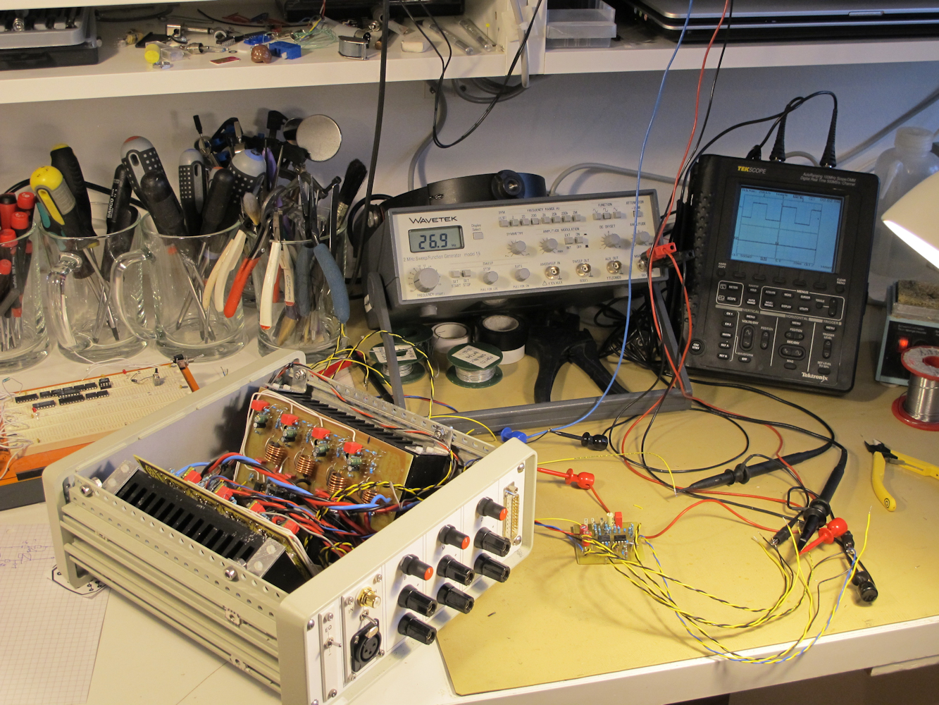


Bild 1.jpg

Sending a picture from my primitive old school desk.


/ Bo Thuné, Linköping, Sweden
 

ZolaIII

Major Contributor
Joined
Jul 28, 2019
Messages
4,196
Likes
2,476
Well it's still the same most part prototyping - testing - modifying circle. Difrence is in a functional prototyping in early before silicon phase which is both time and cost saving. Basically you rute elements and connections they need (whole IC or system block by block) on FPGA (field programmable gate array) and as long array is bigger it will fit in. It's expensive (big fat FPGA's) and used often for verification on complex processes lithography where putting actual silicon on it costs so much that the price of FPGA's and complete verification is tiny.
There are smaller modern FPGA's with application processors (usually couple of ARM core's) that are more adorable and development board's with such.
From there it's to use of lithography specific rooting (layers) libs (including combining couple of them for different elements and D/A) and optimising output even by hand (parametric than auto re rooting). PCB prototyping and optimising and such, actual prototype verification and tuning (including hard revisioning on the hard expensive way when you have to get it on by new silicone print).

Actually current acquisition (in a lack of better word to describe competitive merge behind it) of Xilinx by AMD if finalised will for the first time give us a vendor (still fables one) which will be able to provide vast majority of multi architectural IP's under one roof (with third partys like Synapsys and such).
 
OP
bothu

bothu

Member
Joined
Mar 7, 2021
Messages
88
Likes
335
Location
Linköping, Sweden
Well it's still the same most part prototyping - testing - modifying circle. Difrence is in a functional prototyping in early before silicon phase which is both time and cost saving. Basically you rute elements and connections they need (whole IC or system block by block) on FPGA (field programmable gate array) and as long array is bigger it will fit in. It's expensive (big fat FPGA's) and used often for verification on complex processes lithography where putting actual silicon on it costs so much that the price of FPGA's and complete verification is tiny.
There are smaller modern FPGA's with application processors (usually couple of ARM core's) that are more adorable and development board's with such.
From there it's to use of lithography specific rooting (layers) libs (including combining couple of them for different elements and D/A) and optimising output even by hand (parametric than auto re rooting). PCB prototyping and optimising and such, actual prototype verification and tuning (including hard revisioning on the hard expensive way when you have to get it on by new silicone print).

Actually current acquisition (in a lack of better word to describe competitive merge behind it) of Xilinx by AMD if finalised will for the first time give us a vendor (still fables one) which will be able to provide vast majority of multi architectural IP's under one roof (with third partys like Synapsys and such).
Tank you so much for describing modern design of electronics. The prototyping - testing - modifying circle and hands on still seems to be needed.

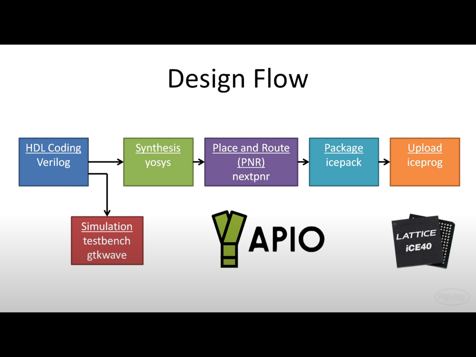
I am 72 years old but still interested in new Technics. I have just started this morning with locking at this clips :


If I had been younger I would have used FPGA solutions instead old gate-logic to get this "field-mouse irritater" working. We have planted 4 new apple trees in the garden and without this "irritator" the field-mouses will eat all the roots of the apple trees.

1.jpg


3.jpg


2.jpg


Best wishes to you.
from Bo Thunér
 
Top Bottom