• WANTED: Happy members who like to discuss audio and other topics related to our interest. Desire to learn and share knowledge of science required. There are many reviews of audio hardware and expert members to help answer your questions. Click here to have your audio equipment measured for free!

made a mistake in my schematic - what is the best option i have?

MCH

Major Contributor
Joined
Apr 10, 2021
Messages
2,659
Likes
2,274
hello guys,
this is just a very short and hope simple question to see if someone can give me some advice.

I am working on a project and when I received the PCBs i realized i had made a mistake:

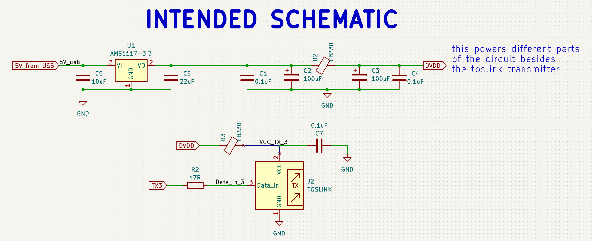
I wanted to assemble a toslink transmitter like this below, that i believe is a very common way (i include the power part of it as it might be relevant to the question):
1690390148440.png


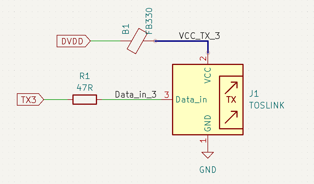
But i forgot, or deleted by mistake, C7, that i believe is there to filter noise from the VCC that supplies the toslink transmitter. What i have on my printed PCB is this:
1690390256625.png


Ok, i think it should not be a big deal, i have other PCBs with toslink transmitters without any filtering in VCC that work fine, but i wanted to know what is the best, or least bad options that i have, also to learn a bit from your answers.

As the PCB is not populated yet, i have some freedom to instead of the ferrite bead B1, place any other part there. With this in mind, i think i could....:

- Place a 0 Ohm resistor instead of the ferrite bead B1 and call it a day, the VCC line already has plenty of filtration.

- Don't worry, add the ferrite bead B1 and forget about the capacitor (this is the option i have more doubts about, i am not sure if the ferrite without capacitor could do more harm than good)

- I could actually solder the capacitor between the VCC and GND pins of the toslink transmitter on the botton side. It will look messy and awful, and might be one day the capacitor just falls off, but i really need this capacitor there and this is definitely the way to go no matter what.

- Other options....

(PS: all the traces are very short, like 2-3 cm maximum from the caps of the 3.3V line filter to the pin of the toslink transmitter)

Thank you for your answers, i appreciate them.
 

Sokel

Master Contributor
Joined
Sep 8, 2021
Messages
6,157
Likes
6,251
It seems as simple as to scrub the trace,cut it and solder the cap.
Except it's in a layer you cant reach.
 
  • Like
Reactions: MCH
OP
M

MCH

Major Contributor
Joined
Apr 10, 2021
Messages
2,659
Likes
2,274
Thanks @Sokel I had not considered that possibility, but unfortunately i don't have space enough between the ferrite bead and the toslink transmitter:

1690392347637.png

This is the top layer. The yellow line is the footprint of the transmitter. B12 is 0805, i can't solder smaller.
 

Sokel

Master Contributor
Joined
Sep 8, 2021
Messages
6,157
Likes
6,251
Isn't C7 after the ferrite going to ground?
 

DVDdoug

Major Contributor
Joined
May 27, 2021
Messages
3,038
Likes
4,005
I would just try without it.

Sometimes "extra" filter & bypass capacitors are more like insurance so maybe if you manufacture lots of boards, a few won't work, etc.

I am working on a project and when I received the PCBs i realized i had made a mistake:
I've worked in electronics a LONG time (not as a PCB designer). I don't think I've ever seen a board come back perfect the 1st time!

I've have made a couple of simple boards for hobby projects and although I was super-careful and double-checked, there were still mistakes. I was super-disappointed but not THAT surprised... I was mentally and financially prepared for a failure on the 1st try. The 1st board was super-simple but the boards were unusable so I had to correct and re-order. The 2nd project was more complicated but still pretty simple (about 25 thru-hole components, no surface mount) and I was able to make it one "work". But I'll be fixing it and re-ordering it too, since I'll be building more than one and I don't want them to be "messy".
 
  • Like
Reactions: MCH
OP
M

MCH

Major Contributor
Joined
Apr 10, 2021
Messages
2,659
Likes
2,274
I would just try without it.
And what of the options would you try first? :D
Sometimes "extra" filter & bypass capacitors are more like insurance so maybe if you manufacture lots of boards, a few won't work, etc.


I've worked in electronics a LONG time (not as a PCB designer). I don't think I've ever seen a board come back perfect the 1st time!

I've have made a couple of simple boards for hobby projects and although I was super-careful and double-checked, there were still mistakes. I was super-disappointed but not THAT surprised... I was mentally and financially prepared for a failure on the 1st try. The 1st board was super-simple but the boards were unusable so I had to correct and re-order. The 2nd project was more complicated but still pretty simple (about 25 thru-hole components, no surface mount) and I was able to make it one "work". But I'll be fixing it and re-ordering it too, since I'll be building more than one and I don't want them to be "messy".
Yes, I also try my best, but s**** happens. Nowadays, the cost is almost nothing, so one would think, bah, just reprint it! But we'll, it is also a matter of waiting a couple of weeks more and well, getting stuff made and shipped from china maybe unnecessarily.... Hm, doesn't make me feel great.
Next time I will try to be more careful, but the balance between "get it finished asap" and "the last double check" is a difficult one for me :)
 

pjug

Major Contributor
Forum Donor
Joined
Feb 2, 2019
Messages
1,776
Likes
1,562
Thanks @Sokel I had not considered that possibility, but unfortunately i don't have space enough between the ferrite bead and the toslink transmitter:

View attachment 301528
This is the top layer. The yellow line is the footprint of the transmitter. B12 is 0805, i can't solder smaller.
Looks like there is room for a cap there, but a bit of a pain. Doing bottom side would be easy, but I don't know if it is a good idea to put a smd part there when plugging into the transmitter might put stress on those pins. Maybe a (thin leads) leaded cap on top side soldered onto pin 2 of B12 and to ground? If you are doing a bunch of these then maybe just redo the pcb.
 
OP
M

MCH

Major Contributor
Joined
Apr 10, 2021
Messages
2,659
Likes
2,274
Put it on it's side angled then to a ground near.
You mean sharing pad 2 with the ferrite bead? Because after the ferrite bead I don't see room enough (remember the yellow line is the physical limit as the toslink will occupy that space)
 

JayGilb

Major Contributor
Joined
Jul 22, 2021
Messages
1,384
Likes
2,356
Location
West-Central Wisconsin
- I could actually solder the capacitor between the VCC and GND pins of the toslink transmitter on the botton side. It will look messy and awful, and might be one day the capacitor just falls off, but i really need this capacitor there and this is definitely the way to go no matter what.
You could glue the cap near the transmitter and solder enameled wire from the cap to VCC and GND.
 
  • Like
Reactions: MCH
OP
M

MCH

Major Contributor
Joined
Apr 10, 2021
Messages
2,659
Likes
2,274
Looks like there is room for a cap there, but a bit of a pain. Doing bottom side would be easy, but I don't know if it is a good idea to put a smd part there when plugging into the transmitter might put stress on those pins. Maybe a (thin leads) leaded cap on top side soldered onto pin 2 of B12 and to ground? If you are doing a bunch of these then maybe just redo the pcb.
Ah true, that might work. Can maybe even reach a ground pad around if the legs of the capacitor are long enough....

Thought the same about the SMD capacitor on the bottom layer, too much stress there, but now I am thinking on a combination with your idea and use a through hole capacitor sharing holes with the toslink. The pins of the toslink are actually super thin.
 
OP
M

MCH

Major Contributor
Joined
Apr 10, 2021
Messages
2,659
Likes
2,274
You could glue the cap near the transmitter and solder enameled wire from the cap to VCC and GND.
Viable option too.
I see almost everyone suggest to keep the cap, I was anticipating the opposite. That will be then.
 
Last edited:

Killingbeans

Major Contributor
Joined
Oct 23, 2018
Messages
4,098
Likes
7,580
Location
Bjerringbro, Denmark.
- I could actually solder the capacitor between the VCC and GND pins of the toslink transmitter on the botton side.

This is what I'd do.

It's not uncommon to see those kind or "post revisions" in PCB production, and using the through hole legs as solder points is probably the most structurally sound solution.
 

Philbo King

Addicted to Fun and Learning
Joined
May 30, 2022
Messages
669
Likes
877
Is the ferrite bead really necessary? They don't really do much until you get up past dozens of MHz. If the circuit is from an app note on the spec sheet and includes the bead, *maybe* keep it (see the link below).
If not, use a zero Ohm resistor in its place.

Often ferrite beads in series with a dc supply create more problems than they solve.

FYI:
 
Last edited:
  • Like
Reactions: MCH
OP
M

MCH

Major Contributor
Joined
Apr 10, 2021
Messages
2,659
Likes
2,274
Is the ferrite bead really necessary? They don't really do much until you get up past dozens of MHz. If the circuit is from an app note on the spec sheet and includes the bead, *maybe* keep it (see the link below).
If not, use a zero Ohm resistor in its place.

Often ferrite beads in series with a dc supply create more problems than they solve.

FYI:
Thanks for sharing, very interesting indeed. The datasheet of the IC I am using only descibes coax output, which doesn't need VCC.
Actually I plan to use the toslink at 96kHz, what means that the led will be switching at a few MHz rate which I guess is not too fast for the bead to become a problem if used with the cap, but to the point of the article, is it really necessary? No idea, I suspect it isn't.
What seems clear is that I should not use the bead without cap.
Anyways, as the card will have 2 toslink outputs, I might try one with the cap in the bottom layer and the other no cap & no ferrite and see, maybe the veils disappear or something :D
Thanks again for the input, it is being a good learning.
 

JayGilb

Major Contributor
Joined
Jul 22, 2021
Messages
1,384
Likes
2,356
Location
West-Central Wisconsin
Thanks for sharing, very interesting indeed. The datasheet of the IC I am using only descibes coax output, which doesn't need VCC.
Actually I plan to use the toslink at 96kHz, what means that the led will be switching at a few MHz rate which I guess is not too fast for the bead to become a problem if used with the cap, but to the point of the article, is it really necessary? No idea, I suspect it isn't.
What seems clear is that I should not use the bead without cap.
Anyways, as the card will have 2 toslink outputs, I might try one with the cap in the bottom layer and the other no cap & no ferrite and see, maybe the veils disappear or something :D
Thanks again for the input, it is being a good learning.
Nice that you have two toslink outputs to experiment with. I'm guessing it will operate well without a decoupling cap in place.
An interesting experiment would be to try it on various usb power sources and see if it makes a difference.
 
OP
M

MCH

Major Contributor
Joined
Apr 10, 2021
Messages
2,659
Likes
2,274
Nice that you have two toslink outputs to experiment with. I'm guessing it will operate well without a decoupling cap in place.
An interesting experiment would be to try it on various usb power sources and see if it makes a difference.

I plan to check for dropouts crackles or similar, and see how they handle 192kHz. I also have a 2m long noname toslink fiber, well, that sort of things. I don't have the resources nor the knowledge to test much more than that.

192kHz is like 12MHz if i am not mistaken. Vcc is 3.3V. If both configs can transmit 192kHz through the 2 meter line successfully, then i know next time i build this circuit i can save a couple of parts :)
 

Zapper

Addicted to Fun and Learning
Joined
Mar 4, 2023
Messages
608
Likes
837
Thanks @Sokel I had not considered that possibility, but unfortunately i don't have space enough between the ferrite bead and the toslink transmitter:
This is the top layer. The yellow line is the footprint of the transmitter. B12 is 0805, i can't solder smaller.
cap.png

All you have to do is scrape away the solder mask next to the ferrite bead with an Xacto knife, exposing the copper ground plane, then butt the cap up against the ferrite, soldering one side to the ferrite and the other to the gnd plane.

>> - I could actually solder the capacitor between the VCC and GND pins of the toslink transmitter on the botton side. It will look messy and awful, and might be one day the capacitor just falls off, but i really need this capacitor there and this is definitely the way to go no matter what.

That would work too. It won't fall off.

I would add the capacitor. Either method is easy to do. I've hacked many circuit boards this way.
 
Last edited:
OP
M

MCH

Major Contributor
Joined
Apr 10, 2021
Messages
2,659
Likes
2,274
guys, just wanted to say thank you and report back.
Got the through hole capacitors but ended up using the smd ones in between the pins of the toslink transmitter. They fit so well that it was too easy to not to try it:

1691958807155.png

And most important: yes, it works perfectly well :)
 
Top Bottom