• WANTED: Happy members who like to discuss audio and other topics related to our interest. Desire to learn and share knowledge of science required. There are many reviews of audio hardware and expert members to help answer your questions. Click here to have your audio equipment measured for free!

High-powered headphone amps

OP
Ariamella

Ariamella

Member
Joined
Nov 14, 2018
Messages
61
Likes
14
I don't think P113 as-is is going to cut it if you want substantially more output power than the Atom... at 8.66 Vrms into 150 ohms and 5.66 Vrms into 32 ohms, that's not exactly a slouch to begin with. Basically, what you'd want is an output stage with gain running on higher supplies, regulated down to +/-15 V for the opamp (we're only talking a few mA, so 78L15/79L15 series parts would be easily sufficient). The SMPS modules you are using are also available in 24 V, that would be a starting point.
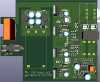
Around as powerful would be fine, I know P113 is capable of 2.2w into 32ohm so that was where I went with it, I just didn't want to downgrade on power. I'll give it a go though!

1. Q1/3 are using the wrong symbol, and Q2/4 are connected wrong entirely.
Whoops, good catch! Fixed.

2. I am not sure whether the simple diode bias circuit is going to get you enough bias... generally you want to be running output transistors like these at 20-30 mA minimum, or else their fT will be competing with a sloth on valium. (Not good for stability. Generally, you want buffer fT >3 * opamp GBW / (noise) gain.) 8 A parts seem a tad oversized in general. I might try some 2SC5200/2SA1943... even the shady second-sourced ones ought to be robust enough for this application. Make sure you get some silpads for mounting, I think those should be adequate in a headphone amp and they're practical and reusable (I doubt there'll be enough heat dissipation to make mica washers worth it).
Fair, I can always go back to the BD139/140s the original design calls for.

3. The two 100 µF capacitors in series can be replaced by a single part across both with no substantial detriment, according to simulation.
That would be, uhh, C3, C4 and C7, C8, right?

4. At lower gains, it is generally advisable to add a small capacitor from opamp output to inverting input, say 22-47 pF, to aid stability. I would consider adding a Zobel network on the output for the same reason. And speaking of gains, having a way of selecting at least two different ones would be good.
If I'm understanding right, that would be between pins 2/6 and 7 for the capacitor? I did see a zobel network mentioned on the P113 page but I didn't think it was necessary. I'll add one.

5. Your secondary-side ground planes have no business being anywhere near mains input nodes - mask out at least 1-2 cm around these areas if you can. You have some reading up on electrical safety and creepage distances to do. What you want is more or less an IEC Class II device. Use heatshrink to cover solder joints, and when mains wiring has to be routed alongside case panels (e.g. for the power switch), use double-insulated mains cable. You always want two layers of insulation between mains and the entire secondary side (a decent distance in air also counts though).
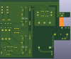
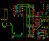
I actually changed the design before seeing this comment because I realized this myself and now the ground plane is only at the secondary side and the amplifier. Take a look at the GitHub! As for the insulation, that makes sense.

6. If a PE connection is commonly available from outlets (I guess Hong Kong uses British plugs?), you can make use of that... use a Y2 rated safety capacitor, ca. 10 nF, to connect incoming PE to chassis ground. Route out a slot in the board underneath the cap, maybe 2-3 mm across and about 1 cm wide. PE can be treated like L and N otherwise. Depending on chassis available, consider an onboard IEC power connector.
No amplifier with unbalanced inputs should have audio ground and PE firmly connected, this is just asking for trouble with ground loops. The Atom is using a transformer plug pack for good reason.
Got it.

Thank you for your advice by the way! This is my first time designing an amp like this so I'm bound to make mistakes.

Edit: modified the schematic! How is it now? Am I right in assuming that the chassis shouldn't be connected to PE at all?
1622123072856.png
 
Last edited:

AnalogSteph

Major Contributor
Joined
Nov 6, 2018
Messages
3,337
Likes
3,278
Location
.de
Edit: modified the schematic! How is it now?
Better. That said -
1. Look where you actually connected C3/C6. That doesn't look like pin 1/7 to me... ;)
2. Switching gain would be likely to create a massive spike on the output as the switch may momentarily not make contact anywhere. You'd better short out a resistor in series or disconnect one in parallel, with values computed as needed (series: 3k3 + (5k6 + 200R), parallel: 9k1 || 5k1).

The output stage still needs to be modified to take advantage of your higher supplies as well. I might consider a CFP output with a bit of gain... not overly much, about 1.8x. It's not the most popular setup, but should work alright if you're mainly in Class A. I'd suggest a transistor bias spreader to go with it. Similar to Fig. 8 here.

You may also require some more effort to keep RFI out, which the LM4562 is notoriously susceptible to. I might consider reducing R2/R12 to 470-510R and adding 470R in series and 220 pF (NP0) to ground at the input ahead of C1/C6. (What type are C1/C6, btw?)

Am I right in assuming that the chassis shouldn't be connected to PE at all?
Yes. This is basically "IEC Class II with benefits". ;)

I hope Kicad has a third "common" symbol to offer. I would suggest using that for the PE then while using the "chassis ground / earth" symbol for the actual chassis connection only. You do want your chassis to connect to circuit ground somewhere, and you'll also have to take care of good electrical connection between case parts (hint: anodized surfaces are not very conductive). Some attention will also have to be paid to where the input jacks will be getting their ground, which will be reflecting in grounding scheme.
 
OP
Ariamella

Ariamella

Member
Joined
Nov 14, 2018
Messages
61
Likes
14
Better. That said -
1. Look where you actually connected C3/C6. That doesn't look like pin 1/7 to me... ;)
Whoops, there we go, fixed! :D

2. Switching gain would be likely to create a massive spike on the output as the switch may momentarily not make contact anywhere. You'd better short out a resistor in series or disconnect one in parallel, with values computed as needed (series: 3k3 + (5k6 + 200R), parallel: 9k1 || 5k1).
Done, used the parallel method as it requires only two resistors and hence less parts.

The output stage still needs to be modified to take advantage of your higher supplies as well. I might consider a CFP output with a bit of gain... not overly much, about 1.8x. It's not the most popular setup, but should work alright if you're mainly in Class A. I'd suggest a transistor bias spreader to go with it. Similar to Fig. 8 here.
That'll probably make the PCB too big to fit in the original case I had in mind. This is quickly becoming a much bigger project than I anticipated! I originally just wanted to miniaturize P113 :p would it work as-is if I used 18v rails instead?

You may also require some more effort to keep RFI out, which the LM4562 is notoriously susceptible to. I might consider reducing R2/R12 to 470-510R and adding 470R in series and 220 pF (NP0) to ground at the input ahead of C1/C6. (What type are C1/C6, btw?)
Done (hopefully as intended). C1/C6 are polypropylene types, they're present on the original circuit I assume to filter out DC offset. I'm planning on switching to the OPA1652 or OPA1642, would that still require more care taken to reduce RFI?

Yes. This is basically "IEC Class II with benefits". ;)

I hope Kicad has a third "common" symbol to offer. I would suggest using that for the PE then while using the "chassis ground / earth" symbol for the actual chassis connection only. You do want your chassis to connect to circuit ground somewhere, and you'll also have to take care of good electrical connection between case parts (hint: anodized surfaces are not very conductive). Some attention will also have to be paid to where the input jacks will be getting their ground, which will be reflecting in grounding scheme.
Yeah, they do. And yeah, when putting together amps before I always scraped part of the anodizing/paint off and then used a multimeter to confirm that they were connected.
 
Last edited:

solderdude

Grand Contributor
Joined
Jul 21, 2018
Messages
15,891
Likes
35,912
Location
The Neitherlands
I thought you didn't like a electrolytic in the output yet you are using a 100uF not even properly biased electrolytic in the feedback path.

Why not change the output path for something like a diamond buffer and use DC servo and get rid of the 100uF.
I see no DC protection on the output which may be a good idea.
 
Last edited:
OP
Ariamella

Ariamella

Member
Joined
Nov 14, 2018
Messages
61
Likes
14
I thought you didn't like a electrolytic in the output yet yet you are using a 100uF not even properly biased electrolytic in the feedback path.

Why not change the output path for something like a diamond buffer and use DC servo and get rid of the 100uF.
I see no DC protection on the output which may be a good idea.
That would be modifying the design too far and then it wouldn't be a P117 anymore...my goal out of this wasn't to make something for myself to build (edit: as I've decided on the X-Altra HPA-1 http://hifisonix.com/hpa-1-class-a-headphone-amplifier/), it's more like a design exercise lol, its also the reason I didn't want to use complimentary pairs in the output

For reference, this is the original schematic:
1622185097041.png
 
Last edited:

solderdude

Grand Contributor
Joined
Jul 21, 2018
Messages
15,891
Likes
35,912
Location
The Neitherlands
You can improve the FB circuit by putting an extra C2 in anti-parallel.

Also I would Use C3+C4 as per this schematic not just 1 between the B of the output stage.
Also You do realize that the LM4562 and the ones you plan to use will not survive the planned 24V. Keep it below 17V or use an opamp that can handle the voltage.

How do you plan to optimally bias the output stage. The rather high emitter resistors will create XO distortion at lower impedance loads as the complementary transistor will switch off completely.
 
Last edited:
OP
Ariamella

Ariamella

Member
Joined
Nov 14, 2018
Messages
61
Likes
14
You can improve the FB circuit by putting an extra C2 in anti-parallel.

Also I would Use C3+C4 as per this schematic not just 1 between the B of the output stage.
Also You do realize that the LM4562 and the ones you plan to use will not survive the planned 24V. Keep it below 17V or use an opamp that can handle the voltage.

How do you plan to optimally bias the output stage. The rather high emitter resistors will create XO distortion at lower impedance loads as the complementary transistor will switch off completely.
Steph recommended an additional voltage regulator to power the opamps instead of the main circuit, though I'm honestly thinking of just changing to +-18V rails and using an OPA1652.

I'm not sure, I have little experience with amplifier design, I was thinking just lower the value of the emitter resistors though.
 
Last edited:

solderdude

Grand Contributor
Joined
Jul 21, 2018
Messages
15,891
Likes
35,912
Location
The Neitherlands
lowering the values of the emitter resistors will:
A: increase the idle current
B: may blow up the output stage due to thermal runaway.

Since you are using opamps anyway I would suggest to use an opamp buffer as output stage. this is far better than bd139/140

Or maybe use an OPA551 with 2x gain which can run on +/-30V and has 250mA output current.
These work fine (used them this way in the Polaris)

Steph's idea works as well and may have benefits over just using a lower PS voltage.

Also I would suggest adding DC protection.
 
Last edited:
OP
Ariamella

Ariamella

Member
Joined
Nov 14, 2018
Messages
61
Likes
14
I don't wish to modify the original circuit too much as it would mean I'd be creating a completely new amp and if I'm doing that, might as well start from scratch

Wonder how much I can lower the emitter resistors before that starts to be a problem (with adequate heatsinking ofc)

It's definitely easier to stick with the original 15V dual rail supply but it would also be possible to use a different smps unit for +-18V.

Edit: well, I uploaded a new version. Hope it's more acceptable.
 
Last edited:
OP
Ariamella

Ariamella

Member
Joined
Nov 14, 2018
Messages
61
Likes
14
Thought I'd post an update.
  • I downloaded LTspice and have been learning how to use it.
  • 47pF miller compensation capacitor helped tame ringing on square waves with a 600R load with 10nF in parallel.
  • A 10R/100nF zobel network has also been added.
  • C2 has been removed. Not sure what it's for.
  • New layout with (hopefully) accurate measurements as drawings of case to be used have been received.
  • Changed PSU to RAC20-15DK to save space and removed varistor.
  • 200mA fuse on-board fuse.
  • Output BJTs changed to MJE15028/29s as they offer slightly better simulated distortion.
  • The gain resistors have been changed to 560R/5k6 to allow for gain values of 1.5 and 6.6.
  • PSU filter has been changed to CLC as that is more than adequate filtering.
  • The DC protection and muting circuit from AMB has been added to protect the headphone out.
  • On-board Y2 capacitor has been added for convenience.
  • Added gain switches.
  • Edit: added RFI RC filter at the last second.
What do you guys think? :)
 

Attachments

  • Render_Top.png
    Render_Top.png
    109.1 KB · Views: 158
  • Render_Bottom.png
    Render_Bottom.png
    45.4 KB · Views: 107
  • PCB_Traces.png
    PCB_Traces.png
    109.4 KB · Views: 199
  • Schem.png
    Schem.png
    81.2 KB · Views: 181
Last edited:

JohnYang1997

Master Contributor
Technical Expert
Audio Company
Joined
Dec 28, 2018
Messages
7,175
Likes
18,292
Location
China
I thought the current gain of the output transistor would be too low. Turns out the 100uF AC path works quite nicely.
 
Last edited:
OP
Ariamella

Ariamella

Member
Joined
Nov 14, 2018
Messages
61
Likes
14
Now, eventually it's not a high power head amp anymore is it? Paralleled opa1656 is probably better with rail to rail output.
Simulated 2.75W into 32R, 0.146W into 600R output is pretty decent if you ask me. :p
 
Top Bottom