• WANTED: Happy members who like to discuss audio and other topics related to our interest. Desire to learn and share knowledge of science required. There are many reviews of audio hardware and expert members to help answer your questions. Click here to have your audio equipment measured for free!

Multichannel audio on a Pi will get a whole lot easier and cheaper!

Hi, for people that also want to get an new 12Bit Scope and like me not sure to get the Siglent SDS1000X HD
or Rigol DHO1000 Series because off the Bode Plot capabillity of the Siglent one Rigol dont has.
here is an nice Post about how to make it with Rigol 12Bit scope and an Siglent Funktiongenerator with Python Script ;)
https://www.eevblog.com/forum/testg...opes-launched-in-china/msg5572791/#msg5572791

The Rigol has Time Base Accuracy ±1.5 ppm ± 1 ppm/year (HDMI OUT, 10MHz Clock IN and Out and better Screen Reselution) while the
Siglent has only Time base Accuracy ±25ppm (but optional 16Channel Logic Analyzer and 20MHz Signalgenerator) and probably also less Bandwith (Hacked)

Siglent writes on his Datasheet:
Noise floor*2 (rms, @50 Ω, typical,1 mV/div) 70 μV(Full Bandwith)

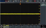
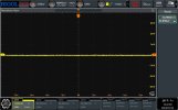
With 50Ohm Termination i measured 63uV @full BW and
25uV @ 20MHz BW Limit AC RMS on Rigol ;)

The Options was not importand for me have them Standalone so i Choose the Rigol from Saelig for 899$ without Shipping, around 1180€ ($990.55 + TAX) all Inclusive to Germany.
because Batronix dont has it on Stock (DHO1074)
https://www.batronix.com/versand/oszilloskope/Rigol-DHO1074.html

Robert
 

Attachments

  • DHO1074_50Ohm CH1 noise full BW.jpg
    DHO1074_50Ohm CH1 noise full BW.jpg
    254 KB · Views: 40
  • DHO1074_50Ohm CH1 noise 20MHz BW.jpg
    DHO1074_50Ohm CH1 noise 20MHz BW.jpg
    232 KB · Views: 36
Last edited:
@Frunse :D
I got a Focusrite Scarlett 18i20 Gen3 on saturday. While reading the manual I realized it supports dual ADAT input and output.
It can handle 8 input channels at 24-bit/96kHz via dual ADAT.
Now I'm looking for a solution to convert 4x I²S from the HDMI audio-extractor to SMUX II. ;)

An alternative route would be HDMI audio-extractor -> 4x I²S -> RasperryPi 5 -> USB -> Focusrite Scarlett 18i20 -> headphones/power-amplifier.
Thats how i made it with the MotuUL MK5 .

Sorry for the Delay with my I2S Project but i didn't forget it, still need it too with the I2S 4CH MUX and an ASRC or software contron on script for Camilla.

But will build both Options to compare it.

Not sure when it could happen but my Amp Project is ready soon i hope.

Robert
 
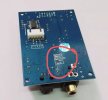
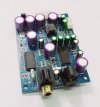
Hi @mdsimon2 and hi @phofman, I'm coming back to an old question. I'm asking you guys, as you've been a lot on this topic: Is there any chance, that by now there is a solution to connect three DAC's directly via I2S to the Raspberry Pi5 for the use with CamillaDSP? Last time we talked about this, I remeber the challenge was to provide 3x MCLK to the GPIO ports. Is there any solution that would allow this by now? I'd like to connect 3x Lampucera DAC boards via I2S directly to the Raspi5 GPIO out pins. Lampucera DAC boards now have a dedicated mark of the required I2S pins (see attached pics). It would be great, if I could skip the I2S to SPDIF conversion in stick to I2S completely. For audio in, I currently use Wiim Pro Plus optical out to a optical SPDIF to USB converter (once the new Wiim Ultra is available on the German market, I would move to this, in order to be able to use the USB out directly into the Raspi).
 

Attachments

  • s-l1600.jpg
    s-l1600.jpg
    82.7 KB · Views: 50
  • s-l1601.jpg
    s-l1601.jpg
    260.6 KB · Views: 51
Hi guys,

In case someone was following, just wanted to make you aware that I am about to give up with the multichannel HDMI input hat project.
I designed and printed the PCBs, that I am very happy with and look great. I eventually made them 6 layers because JLCPCB offered to make them for free, but needed to be 6 layers, so I did signal/ground/power/signal/ground/signal.
1724684861164.png

Of course I made a couple of mistakes but fortunately I realized before finishing and could correct them with a couple of tiny jumpers (I used a footprint that was not correct for a couple of mosfets that interface the 5V HDMI SDA/SCL pins to 3.3V of the extractor chip), as you can see in the picture close to the input connector.
1724684777227.png
1724684144430.png

These are the hats partially populated, but that should be functional.
Definitively this is not a project for a first time soldering SMD, there are 0402 parts and the main chip has 128 pins, but if you have some practice is perfectly doable:

What happened then? Well, it does not want to boot up. I am almost certain it is a problem with the internal MCU, that somehow got its program corrupted. I read in the internet that programmed chips can survive soldering but the problem here is that you need to heat A LOT the chip to desolder it from the donor board, as the PCB itself is very big with ground pours and unleaded solder…. I am pretty sure that the chip got damaged at that stage.

What happens is that when I power the board, all the LEDS light (like in the original device), but stay lite (unlike the original device). Additionally, 12MHz the master clock signal is not there, unlike in the original device where it is always present, and the i2s signals don’t show up when they should. The only other external signal that measures different to the original device is hto_ctlb (no idea what that means) that should go low to activate a mosfet that turns HEAC- low (if I bring that pin down manually nothing changes). Other than that, all power pins have power and there are no bridges or bad contacts in any of the 128 pins, that I checked one by one…. :-/

Fortunately I spent next to no money in this project, as I reused all the parts except the crystal, but I did spend a lot of hours on it, so I will leave it in the drawer for a while. If I ever come across one of these extractors for a good price, I might buy one and try to desolder the chip differently, with some of that liquid metal or just cutting the PCB so that the thermals are more favorable, but I don’t want to risk burning another IC....
 
Last edited:
Hi guys,

In case someone was following, just wanted to make you aware that I am about to give up with the multichannel HDMI input hat project.
I designed and printed the PCBs, that I am very happy with and look great. I eventually made them 6 layers because JLCPCB offered to make them for free, but needed to be 6 layers, so I did signal/ground/power/signal/ground/signal.
View attachment 388622
Of course I made a couple of mistakes but fortunately I realized before finishing and could correct them with a couple of tiny jumpers (I used a footprint that was not correct for a couple of mosfets that interface the 5V HDMI SDA/SCL pins to 3.3V of the extractor chip), as you can see in the picture close to the input connector.
View attachment 388620View attachment 388615
These are the hats partially populated, but that should be functional.
Definitively this is not a project for a first time soldering SMD, there are 0402 parts and the main chip has 128 pins, but if you have some practice is perfectly doable:

What happened then? Well, it does not want to boot up. I am almost certain it is a problem with the internal MCU, that somehow got its program corrupted. I read in the internet that programmed chips can survive soldering but the problem here is that you need to heat A LOT the chip to desolder it from the donor board, as the PCB itself is very big with ground pours and unleaded solder…. I am pretty sure that the chip got damaged at that stage.

What happens is that when I power the board, all the LEDS light (like in the original device), but stay lite (unlike the original device). Additionally, 12MHz the master clock signal is not there, unlike in the original device where it is always present, and the i2s signals don’t show up when they should. The only other external signal that measures different to the original device is hto_ctlb (no idea what that means) that should go low to activate a mosfet that turns HEAC- low (if I bring that pin down manually nothing changes). Other than that, all power pins have power and there are no bridges or bad contacts in any of the 128 pins, that I checked one by one…. :-/

Fortunately I spent next to no money in this project, as I reused all the parts except the crystal, but I did spend a lot of hours on it, so I will leave it in the drawer for a while. If I ever come across one of these extractors for a good price, I might buy one and try to desolder the chip differently, with some of that liquid metal or just cutting the PCB so that the thermals are more favorable, but I don’t want to risk burning another IC....
I was keeping an eye on this ... sad to hear the chip died. You definitely need a hot air gun for this kind of desoldering - it's the only reliable way.
 
  • Like
Reactions: MCH
I was keeping an eye on this ... sad to hear the chip died. You definitely need a hot air gun for this kind of desoldering - it's the only reliable way.
Thank you gordoste. I did use a hot air gun, and being my first time desoldering ICs, probably my technique is not the best. The problem is that the PCB is too big and the pins can dissipate a lot of heat, most especially the gnd ones, while the body of the chip no so much, so to bring the pins to temperature is very difficult and you end up overheating the chip itself. That's why I think a good option in this case is to cut out the part of the PCB where the chip is so that you don't need so much energy to reach the melting temperature of the solder.
And now I understand why when they show the people recovering parts from old computers in documentaries, the first thing they do is to cut the motherboard in small parts. Sadly, they know what they are doing...
Tbh I wasn't expecting this to be a problem and didn't do the necessary research beforehand.
 
@MCH: Another option is using a low-temperature metal, e.g. safe http://www.chipquik.com/store/index.php?cPath=600_630 or non-ecological https://www.ebay.com/itm/204495079552 . You just melt the metal onto the pins and spread around the chip, mixing the low-temp metal with the solder metal, using a lot of solder flux. I (very occasionally) use the woods metal which melts at some 70 centigrades, the mix stays liquid for many seconds. After removing the chip you need to clean the pads with solder wick and dispose of the remains. No danger of damaging the board.
 
  • Like
Reactions: MCH
I am not personally very interested in multichannel I2S output but I figured others might be (although I always love to tinker). And as a first step in multichannel I2S with the RPi I figured multichannel output would have less variables as I already have a McFIFO / McDualXO + 8 channel AES output device sitting on the shelf that I know works with multichannel I2S input.

I am mostly interested in the potential for multichannel I2S input from a 7.1 HDMI to I2S extractor like this -> https://www.aliexpress.us/item/2251832845605595.html. An Apple TV + HDMI to I2S extractor + RPi 5 running CamillaDSP + multichannel USB DAC (like the UL Mk5) is a very interesting AVR replacement setup to me.

Michael
Hi everyone. As you may know, I am planning on using this board with an Apple TV, but have recently decided to dust off my blu-ray player. So now, I have two HDMI sources which I can mux with a switcher. The question I now have is whether the blu-ray player outputs unencrypted PCM like the Apple TV. From reading the specs it seems like it might, does everyone else have the same interpretation? specs here: https://www.lg.com/uk/video/blu-ray...K5hi7KycGpFohwFnEFVvmf7YNIWss1kVyK1uy8_EuF7yE (Audio Features). The model is LG Blu-Ray/DVD Player BP-240.
 
Hi everyone. As you may know, I am planning on using this board with an Apple TV, but have recently decided to dust off my blu-ray player. So now, I have two HDMI sources which I can mux with a switcher. The question I now have is whether the blu-ray player outputs unencrypted PCM like the Apple TV. From reading the specs it seems like it might, does everyone else have the same interpretation? specs here: https://www.lg.com/uk/video/blu-ray...K5hi7KycGpFohwFnEFVvmf7YNIWss1kVyK1uy8_EuF7yE (Audio Features). The model is LG Blu-Ray/DVD Player BP-240.
Never mind, should have just read the manual!
 

Attachments

  • bp240_audio_menu.png
    bp240_audio_menu.png
    358.1 KB · Views: 36
Another option would be an SBC with a SoC which already integrates the HDMI receiver. E.g. Khadas VIM4 with Amlogic A311D2 or the many SBCs with full-version RK3588.

In my tests RK3588 runs 4k/60Hz youtube video from my PC second HDMI out -> HDMI IN -> playback app -> 4k/60Hz HDMI OUT -> 4k/60Hz monitor clean, passive cooling no heatsink. HDMI audio interfaces are internal I2S interfaces handled by standard alsa devices (8ch capture for HDMI RX, 8ch capture + 8ch playback for HDMI TX + eARC). The RK3588 support gradually reaches mainline kernel https://gitlab.collabora.com/hardwa...-rockchip-3588/-/blob/main/mainline-status.md , my tests were on some android kernel with full HW support.

That SoC has a number of external I2S interfaces, most of which are not available on the 40-pin headers of the standard SBCs. But building an IO board for one of the RK3588 compute modules available would allow using most of the many I/O interfaces that powerful 8nm SoC offers. Such board would require just a few active components, but lots of precise differential pairs, ESD protections, and lots of useful connectors. Running Pipewire (+ e.g. CDSP) multi-routing between all the available I/O audio/video interfaces (including USB gadget, BT, network streams, etc etc - all of that already is supported by pipewire). Doing audio DSP for video passthrough HDMI I -> O. IMO that is the way for the future.

I'm considering using a RK3588 board instead of the eARC->HDMI extractor + HDMI->I2S extractor combo, and on paper it looks like using such board as an input for the I2S on RPi5 should work. I would also need to add some kind of I2S->SPDIF transceiver to clock the external DAC, but that should be solvable too.

The only thing that bothers me is having to use two SBCs. Perhaps RK3588 allows to clock the external DAC from the eARC input somehow without having to output to I2S?
 
Because I don't see how I could output the audio from the RK3588 directly to a USB DAC, and at the same time clock that DAC from the eARC input. Going through the I2S allows to hook up in parallel an SPDIF transceiver for the clocking purpose, but if everything could be done using a single SBC, that could indeed be the perfect all-on-one solution.
 
The datasheet does not talk about the internal I2S clock i2s9_sclk/i2s10_sclk being available outside of the SoC. The standard solution would be to adaptively resample the input signal to the output clock, e.g. using camilladsp.
Nevertheless such project with RK3588 would require a major kernel configuration and probably hacking as not all of the features are already ported from the old android kernel.

With RPi5 only some eARC->I2S convertor would be needed + slaving both input and output I2S interfaces to the incoming I2S clock.
 
Some cheapo eARC extractors have the i2s pins quite accessible, if someone feels adventurous...:

 
Some cheapo eARC extractors have the i2s pins quite accessible, if someone feels adventurous...:

This one even has already populated pins for each of the 4 stereo pairs. No eARC though but it can be daisy chained after an eARC to HDMI box.


I explored this board to convert from HDMI to I2S and then to an SBC or PC where I could process the audio but never got to find a reliable I2S input mechanism.

My use case was a bit of a “spent so much time figuring out how to do it that never stopped to think if I should be doing it”.
I wanted to connect a Nintendo Switch to it, capture the I2S data and encode on the fly to either Dolby or DTS so I could connect to an old receiver that doesn’t have HDMI inputs.
All this to play Zelda and Mario Kart 8 with surround sound . I know, I’m cheap and don’t want to buy a new receiver just for the Switch.
 
capture the I2S data and encode on the fly to either Dolby or DTS so I could connect to an old receiver that doesn’t have HDMI inputs.

All this to play Zelda and Mario Kart 8 with surround sound
For such usage the latency of the added chain may not be negligible.
 
For such usage the latency of the added chain may not be negligible.
Agreed. Although I’ve recently discovered that most sound bars have latencies between 30-150ms and I don’t see everyone complaining about it (based on rtings.com measurements). But you are correct. The latency and possible stability issues might not be worth it but never got to confirm by myself.
 
Back
Top Bottom