
Understanding FPGAs
FPGAs have become part of the parlance of DAC technology so I thought I write this article to explain what they are.
Before we understand FPGAs we need to first learn a bit about digital circuits. Digital circuits used to be designed using discrete tubes and then transistors. Later, Integrated Circuit (ICs) were invented that could contain blocks of transistors and other components. This led to creation of specific ICs that performed digital logic operation. There were too types of these, TTL and CMOS but both accomplished the same thing. They provided basic logic circuits such as AND, OR, Counters, etc. Much more complicated digital circuits could now be designed by using ICs. Less space was taken and designs simplified.
IC revolution also gave birth to Microprocessors which power so much of our life today from computers to smartphones. This provided another path to get digital work done. Instead of designing fixed function circuits, a computer is a general purpose machine where the program written for it performs the function. To add numbers, you tell the microprocessor to do that for you. By changing the program, you change the operation of a digital computer. That flexibility came with a price: much slower speed. Today’s microprocessors are incredibly fast so that is not as much of an issue for many problems but all else being equal, a circuit designed using logic building block will be faster and more efficient.
Another way to skin the cat was through what is called an ASIC which is short for Application Specific Integrated Circuit. An ASIC is a (larger) cluster or digital circuits customized for a specific function. Being a custom implementation, an ASIC can be incredibly fast, and power efficient. And on a per unit basis, can be cheaper than other solutions. On the negative side, ASICs are very difficult to design and require high-up front expense. Non-recurring Engineering (NRE) fee may run into a million dollars. Worse yet, if you make a mistake, you may have to pay some of that again to “spin” the ASIC and make a new revision that works. For these reasons ASICs are justified for very high volume products where the NRE and engineering costs can be amortized over that volume and performance advantages realized.
All of this gets us to FPGAs. What if we could have the programmability of microprocessors, yet speed of ASICs? That is more or less what we have in FPGA or Field Programmable Gate Arrays. An FPGA is designed somewhat like an ASIC but unlike an ASIC, it can be erased and reprogrammed. Making a mistake now is no big deal. Simply change the design and re-download into the FGPA. Indeed, the typical design for a system with an FPGA is to store its program in flash memory and upon powering up the device, the program is pushed into the FPGA. This allows “software” updates of FPGA.
Note that FPGAs are still complex to design. Not as bad as ASIC but still, far more difficult than writing a computer program. They also require specialized tools to program. As such, they are outside of DIY skills. It requires a proper digital designer to program one.
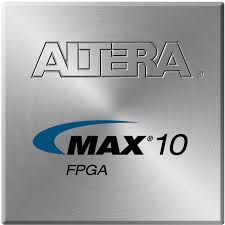
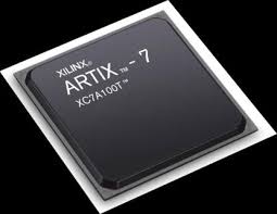
Leading suppliers of FPGAs by far are Altera and Xilinx. So any time you see those names on a part on a circuit board, you know right away that there is an FPGA there.
Here is an example of the Intona USB isolator. The Xilinx FPGAs are clearly visible.

Traditionally FPGAs were smaller and much slower than ASICs. Today if you have the money, you can buy very large FPGAs but each may cost you $1,000 or more. If you are building high-end products, this can be justified. In exchange for the dollars spent, you get to have full custom solution. You want to add 48 bit numbers? You can do that in an FPGA. Same operation in a computer program would require you to either operate in 32 or 64 bits. FPGAs therefore allow more efficient implementation of a logic circuit but at much higher cost of development.
Realizing some of the drawbacks of FGPAs, the vendors now provide them with embedded (ARM) CPUs and memory. Those components allow you to mix both technologies. Use the CPU for non-math-intensive operation such as control (i.e. what to do) and use the rest of the FPGA for fast and efficient customization.
On the other hand, computers bring so much computing power to us that one can use them in a wasteful manner and still perform the job. Better yet, they have huge amount of high-performance memory which FPGAs by themselves don’t have. Hence the recent development of software upsampling logics such as HQPlayer. If you are OK with maintaining a computer instead of buying a dedicated piece of hardware with FPGA that “just works,” then provide a reasonable alternative.
FPGAs have become part of the parlance of DAC technology so I thought I write this article to explain what they are.
Before we understand FPGAs we need to first learn a bit about digital circuits. Digital circuits used to be designed using discrete tubes and then transistors. Later, Integrated Circuit (ICs) were invented that could contain blocks of transistors and other components. This led to creation of specific ICs that performed digital logic operation. There were too types of these, TTL and CMOS but both accomplished the same thing. They provided basic logic circuits such as AND, OR, Counters, etc. Much more complicated digital circuits could now be designed by using ICs. Less space was taken and designs simplified.
IC revolution also gave birth to Microprocessors which power so much of our life today from computers to smartphones. This provided another path to get digital work done. Instead of designing fixed function circuits, a computer is a general purpose machine where the program written for it performs the function. To add numbers, you tell the microprocessor to do that for you. By changing the program, you change the operation of a digital computer. That flexibility came with a price: much slower speed. Today’s microprocessors are incredibly fast so that is not as much of an issue for many problems but all else being equal, a circuit designed using logic building block will be faster and more efficient.
Another way to skin the cat was through what is called an ASIC which is short for Application Specific Integrated Circuit. An ASIC is a (larger) cluster or digital circuits customized for a specific function. Being a custom implementation, an ASIC can be incredibly fast, and power efficient. And on a per unit basis, can be cheaper than other solutions. On the negative side, ASICs are very difficult to design and require high-up front expense. Non-recurring Engineering (NRE) fee may run into a million dollars. Worse yet, if you make a mistake, you may have to pay some of that again to “spin” the ASIC and make a new revision that works. For these reasons ASICs are justified for very high volume products where the NRE and engineering costs can be amortized over that volume and performance advantages realized.
All of this gets us to FPGAs. What if we could have the programmability of microprocessors, yet speed of ASICs? That is more or less what we have in FPGA or Field Programmable Gate Arrays. An FPGA is designed somewhat like an ASIC but unlike an ASIC, it can be erased and reprogrammed. Making a mistake now is no big deal. Simply change the design and re-download into the FGPA. Indeed, the typical design for a system with an FPGA is to store its program in flash memory and upon powering up the device, the program is pushed into the FPGA. This allows “software” updates of FPGA.
Note that FPGAs are still complex to design. Not as bad as ASIC but still, far more difficult than writing a computer program. They also require specialized tools to program. As such, they are outside of DIY skills. It requires a proper digital designer to program one.
Leading suppliers of FPGAs by far are Altera and Xilinx. So any time you see those names on a part on a circuit board, you know right away that there is an FPGA there.
Here is an example of the Intona USB isolator. The Xilinx FPGAs are clearly visible.
Traditionally FPGAs were smaller and much slower than ASICs. Today if you have the money, you can buy very large FPGAs but each may cost you $1,000 or more. If you are building high-end products, this can be justified. In exchange for the dollars spent, you get to have full custom solution. You want to add 48 bit numbers? You can do that in an FPGA. Same operation in a computer program would require you to either operate in 32 or 64 bits. FPGAs therefore allow more efficient implementation of a logic circuit but at much higher cost of development.
Realizing some of the drawbacks of FGPAs, the vendors now provide them with embedded (ARM) CPUs and memory. Those components allow you to mix both technologies. Use the CPU for non-math-intensive operation such as control (i.e. what to do) and use the rest of the FPGA for fast and efficient customization.
On the other hand, computers bring so much computing power to us that one can use them in a wasteful manner and still perform the job. Better yet, they have huge amount of high-performance memory which FPGAs by themselves don’t have. Hence the recent development of software upsampling logics such as HQPlayer. If you are OK with maintaining a computer instead of buying a dedicated piece of hardware with FPGA that “just works,” then provide a reasonable alternative.
Last edited:
