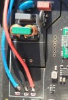
So guys! Let's take apart a node called Ultra -Low Noise Power Supply ±12V 1A. And why you need to get rid of it immediately). What is this expanded block? If we turn on the X-ray vision and make some effort, we will find a handkerchief with details under the layer of compound and metal.
View attachment 545910
Upon closer examination, we realize that this is a conventional single-cycle flyback switching power supply (Flyback SMPS). Hmm! Let's take a look at its output stage circuit.
View attachment 545911
To the moderator! change the text to "What has this clever Chinese hand done here?"? This is a classic example of Chinese engineering magic (or cost-saving), which is called a floating output circuit (bipolar power supply without a transformer midpoint). Here's what we have on the secondary side:
1. There are three tracks leading from the encapsulated block (transformer) to the main board. (+12V, -12V, GND)
2. The +12 V* line is rectified directly on this board by the dual Schottky diode D5 and smoothed by the capacitor C60 relative to GND.
The -12 V* line (pin 5) goes "raw" to the DAC motherboard. This is how it works and no other way.
Then the question arises: how is the negative voltage generated? Let's take a closer look at the DAC board
View attachment 545914
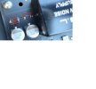
What is it. Ha! It turns out that our Chinese magicians have installed 2 elements: the first is a SS520 Schottky rectifier diode, 200V, 5A, and the second is a KX 2204 suppressor. The circuit diagram is as follows
View attachment 545915
Now we understand how negative voltage is formed. But! The question arises, why is there a suppressor here? And here is the “magic” )) Anyone who has updated the firmware on this device at least once has turned it into the factory bootloader mode. What happens in this mode is that the microcontroller cuts off everything that gets in its way for a full-fledged firmware, as it is a power-consuming mode that disables the peripherals. At this point, the load on the +12V line drops dramatically. We return to the circuit of a single-cycle flyback switching power supply (Flyback SMPS) and here we are faced with the main inherent defect of budget flyback (Flyback) power supplies with multiple outputs. When the load on the +12V shoulder drops, the voltage on the -12V shoulder shoots up to 18V and higher up to 25V:
Why is this happening?
The feedback only monitors one channel:
The feedback circuit (via a optocoupler) on this board only monitors the +12V voltage. The PWM chip doesn't know anything about the -12V channel, as it doesn't have eyes on that side.
What happens when the +12V load is removed:
When the positive load drops (the DAC enters standby mode or a stage is disabled), the C60 capacitor stops discharging. The voltage on it tries to grow, for example, to 12.1 V.
The PWM controller's reaction:
The photocoupler immediately sends a signal to the chip on the primary side: "Stop, the voltage is rising, reduce the pulse width!" The PWM controller dutifully narrows the pulses to a minimum.
The physics of the transformer (the "pumping" effect):
Since the pulses have become very short, the energy stored in the core decreases. However, the dissipation inductance of the transformer's windings remains unchanged. At the moments of switching the key, there are short, but very powerful parasitic high-frequency emissions (voltage spikes).
Where does the extra energy go:
The +12 V channel is locked by feedback and almost does not consume current. All the energy of these parasitic emissions goes to the -12 V channel. Since the diode works on rectifying the peaks on the minus side, and there is no load there now (or it is minimal), thecapacitor in the -12 V channel begins to work as a peak detector. It greedily absorbs these high-voltage emissions and charges up to 18 Volts.
And at this point, the Suppressor comes on stage and begins to limit the voltage, preventing it from rising above 13-18V. However, our Chinese brothers do not pay much attention to component selection, and this Suppressor begins to operate even in normal mode at 11.8-12.4V, generating severe interference in the line. You can verify this by using a thermal imaging camera. Now the physics of this "Ultra-Low Noise" unit is finally in place. This is not a power supply, but a real time bomb for the audio path of the DAC.
Good luck to everyone!