• Welcome to ASR. There are many reviews of audio hardware and expert members to help answer your questions. Click here to have your audio equipment measured for free!

RP2350 DSP board with AK5534 & AK4458

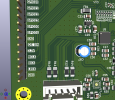
Incidentally there's a similar grid for that location on the bottom mask and paste layers, both on the earlier version and this one. Is that intentional, or did something meant for the top layers end up on the bottom? I only noticed it when I accidentally opened the bottom layer files instead of the top.
Yes, the pad is the primary GND return and is connected to the GND pours on the other layers.
 
sometimes i leave such pad at the oposite side to solder a small heat sink to power mosfets and stuff like that, but i guess that is not the intention and anyways might not be a good idea here. What i see, looks more like vias with a large outer diameter without mask. My only concern there would be if the diameter of the vias is too large, the solder being sucked and the pad left with not enough solder.

One thing that might not be a great idea though is to place C17 and C12 on the back side... probably unimportant but it is often recommended to place those capacitors on the same side of the pins they are connected to (i did not read the hardware guidances so my apologies if they instruct otherwise).

BTW, see how the official pico solves the power rails under the chip, from a promotional picture. IOVDD the outter square and DVDD the inner and vias to the pins:

1786521971715.png
 
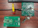
I managed to build and test both boards.
The first version of the Pico board works fine on USB and probably on SPDIF over optical. SPDIF over coax needs the signal amplified to TTL level. I've also tested the MCLK signal from the crystal and it works fine.
The RP2354A also works fine, I have some issues with the MCLK crystal so that needs some sorting out. I haven't populated the ADC yet.
I've also tested control surfaces. I'll probably extend this board to the larger RP2354B and expose more GPIO.
I'm also tempted to remove the ADC entirely and only expose an I2S port where a separate ADC module can be plugged in. That would leave more space for GPIO and I'm not sure how many people would choose an analog input over digital.
The ES9081 was programmed from inside the DSPi firmware, it needs some registers configured. So the board will use a custom built DSPi firmware.
 

Attachments

  • PXL_20260904_091849795.jpg
    PXL_20260904_091849795.jpg
    804 KB · Views: 98
SPDIF over coax needs the signal amplified to TTL level.
There is also S/PDIF output driver inside the ES9081 which you can enable using registers if you have any free GPIO pins left.

Is there any specific reason why you decided to generate MCLK externally using XTAL?

I'm also working on similar board right now but I'm thinking about using internal APLL in ES9081 and in the ADC, with DAC being the master generating BCLK & LRCLK and ADC and DSPi being the slaves.
Potentially APLL should offer superior performance and I would save myself a hassle of routing high speed MCLK all over the whole board.
 
I saw something about SPDIF in the ES9081 but I haven't studied it.
I chose an MCLK crystal because I didn't know if I can trust the one generated by the RP. Also DSPi can only do 256fs, while ES9081 needs 512fs by default. APLL is even harder to configure, but I got that going as well.
What ADC are you using?
 
Texas Instruments TLV320ADC6140 / TLV320ADC5140
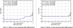
Quad channel ADC with integrated front-end amplifier, THD+N below -110 dB when input signal is kept below -10 dBFS for around 3-4 EUR sounds like good deal.

1788526157258.png
 
I believe that TLV320ADC5140 is a essentially a four-channel version of the TAA512 chip.
At least datasheets and features looks very similar to TAA/TAD/TAC 5xxx family.


It is actually interesting why we are not seeing these chips in for example audio interfaces.
Performance on paper looks very good and BOM cost is dirt cheap.
 
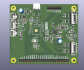
I decided to do an update on this project.
I removed the ADC since it took a lot of board space and instead exposed more GPIO for control surfaces. I also moved to the RP2354B that has more pins.
I2S clock lines and MCLK are also exposed so an external I2S module can be connected. The user can choose between ADC, bluetooth or something else.
I kept the ES9081 DAC as I think it works very well.
There are two SPDIF input ports, one for optical and one for coax. The coax uses the 74LVC2GU04 to amplify the signal.
Power now exclusively comes from USB.
 

Attachments

  • DSPi_MainBoard_RP2354B.png
    DSPi_MainBoard_RP2354B.png
    139.7 KB · Views: 82
Ho deciso di fornire un aggiornamento su questo progetto.
Ho rimosso l'ADC perché occupava molto spazio sulla scheda e ho invece reso disponibili più pin GPIO per le superfici di controllo. Sono anche passato al RP2354B che ha più pin.
Le linee di clock I2S e MCLK sono anch'esse esposte, consentendo il collegamento di un modulo I2S esterno. L'utente può scegliere tra ADC, Bluetooth o un'altra soluzione.
Ho mantenuto il DAC ES9081 perché penso che funzioni molto bene.
Sono presenti due porte di ingresso SPDIF, una per il cavo ottico e una per il cavo coassiale. Per l'ingresso coassiale viene utilizzato il circuito integrato 74LVC2GU04 per amplificare il segnale.
L'alimentazione ora proviene esclusivamente dalla porta USB.

Sto valutando anche il 9081 per le sue eccellenti prestazioni; hai effettuato delle misurazioni in uscita? Stai lavorando a un progetto commerciale o open-source?
 
Sto valutando anche il 9081 per le sue eccellenti prestazioni; hai effettuato delle misurazioni in uscita? Stai lavorando a un progetto commerciale o open-source?
I have only done output level measurements to confirm everything runs fine. I don't have any equipment to do more advanced measurements.
I'm planning on selling these boards eventually but I also have a more DIY version that has the Raspberry Pico.
 
Hi, I’m working on a project to add stereo balanced XLR analog inputs to DSPi running on the Raspberry Pi Pico 2 / RP2350, while retaining its existing DSP features like PEQ, gain, delay, and crossover.

I came across your RP2350 DSP board project using the AK5534 ADC and AK4458 DAC, and I also noticed the discussion mentioning that I2S input was tested with a PCM1808 ADC in master mode at 48 kHz and 96 kHz.

I’d like to understand whether I can use a PCM1808-based ADC module to feed analog XLR audio into DSPi through I2S.

A few questions:

  1. Is I2S ADC input currently supported in the DSPi firmware, or would it require custom firmware?
  2. Can I connect a PCM1808 ADC module to the RP2350 and route its audio into the existing DSP processing chain?
  3. What would be the recommended clocking arrangement for the ADC and RP2350? Would I need an external MCLK, or can the RP2350 handle synchronization?
  4. Is it possible to switch between USB audio, SPDIF, and I2S analog input in the firmware?
  5. Would the current RP2354B board with exposed I2S clock lines and MCLK support this setup?
My goal is to build a stereo analog XLR input → ADC → DSPi processing → DAC output system.

Any guidance on the hardware connections, firmware changes, or existing examples would be greatly appreciated. Thanks!
 
I haven't worked with PCM1808, but:
1. it is supported officially
2. yes
3. typically the DSP acts as the clock master and the ADC as the clock slave. If the ADC needs MCLK, DSPi can provide that
4. yes, I'm using the pushbutton of a rotary encoder to switch between sources
5. I have a new board revision (on post #49) that exposes I2S clock lines, so that any external I2S module can be attached to it

If you use a Raspberry Pico MCU you can connect an ADC module directly to the pins, and maybe some pushbuttons to cycle between sources.
 
Thanks for the reply

I’m planning to use a PCM1808-based stereo ADC module with balanced XLR inputs and connect it to the RP2354B board.

Could you please share the I2S pinout and clock connections for the board revision in post #49? Also, is there any existing DSPi configuration or example showing how to connect an external I2S ADC and enable it as an input source?

Since I’m planning to use the PCM1808, I’d also like to confirm whether it can operate as an I2S slave with the clocks provided by DSPi.

Thanks again!
 
See attached.
 

Attachments

  • Screenshot_20261001_084643.png
    Screenshot_20261001_084643.png
    332.2 KB · Views: 51
  • Screenshot_20261001_084819.png
    Screenshot_20261001_084819.png
    38.7 KB · Views: 58
  • Screenshot_20261001_084956.png
    Screenshot_20261001_084956.png
    38.9 KB · Views: 53
AND ALSO, I have a Focusrite Scarlett 2i2 sound card, and I want to connect its output to the PCM1808 ADC and then to the raspberry pico as suggested.

What circuit should I use between the XLR output of the 2i2 and the analog input of the PCM1808? Do I need any balanced-to-unbalanced/differential receiver or analog conditioning stage?

And also, what is the output signal level of the Focusrite 2i2's XLR line output, and how should I match/condition that signal to the PCM1808's required analog input level/range?

Is there a recommended circuit for connecting the Focusrite 2i2 output directly to the PCM1808?

Thank you!
 
Going ADC --> DAC --> ADC is rarely optimal, need a very clean signal chain for that not to introduce SINAD deterioration
 
Back
Top Bottom