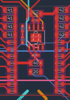
Btw, looking at your preliminary layout, did I just spot a typical error I see that can easily spoil signal integrity? A decoupling cap left and right of the OPA1612, with each one having its own local GND via to the plane. A big no-no. Combine the cap GNDs first, then via down into the plane.

Otherwise you'll have different GND paths for each half-wave of load current (once it's above class-A bias region).
And why does the OPA1612 have a thermal pad when it is SO-8? Only the WSON package has that. That pad gets in the way of the above, as the GND via(s) for the decoupling return should ideally be right under the chip.
EDIT: Or are the two smaller chips at the bottom end two 1612's in WSON? If so, same problem as far as I can see.
Last edited: