deadwood83
Member
- Joined
- Sep 1, 2022
- Messages
- 91
- Likes
- 160
So, back in my early days of being able to afford better gear, I snagged a newly-released Gustard X20 (not the X20u with the USB card). THis unit served me faithfully until about 2019, when I decided that the DX7 Pro was good enough to ditch the HP amp (many) / DAC stack and convert to an AIO unit. At that point, the Gustard was put in a closet where it sat until a few months ago.
I was dead-set on improving a cheap 2x 9038Q2M DAC which measured just above 90dB TD+N. At one point, after frying the USB eeprom with a bad flash I broke out the Gustard and its accompanying Singxer SU-1 so I could use the Singxer to feed LVDS I2S into the cheapie. Once I had taken the cheap DAC from an okayish 91dB TD+N all the way to 108dB TD+N I was fairly satisfied. 108 may sound a little low but we are all spoiled. Everything I measure shows worse results than here so I am guessing it performs quite similarly to a Topping D10 Balanced.
Anyway, since the Gustard was sitting there on the floor I thought "why not?...." and that is how this all began. I failed to capture very detailed measurements because the numbers were disappointing enough I figured it would just go back into the closet.
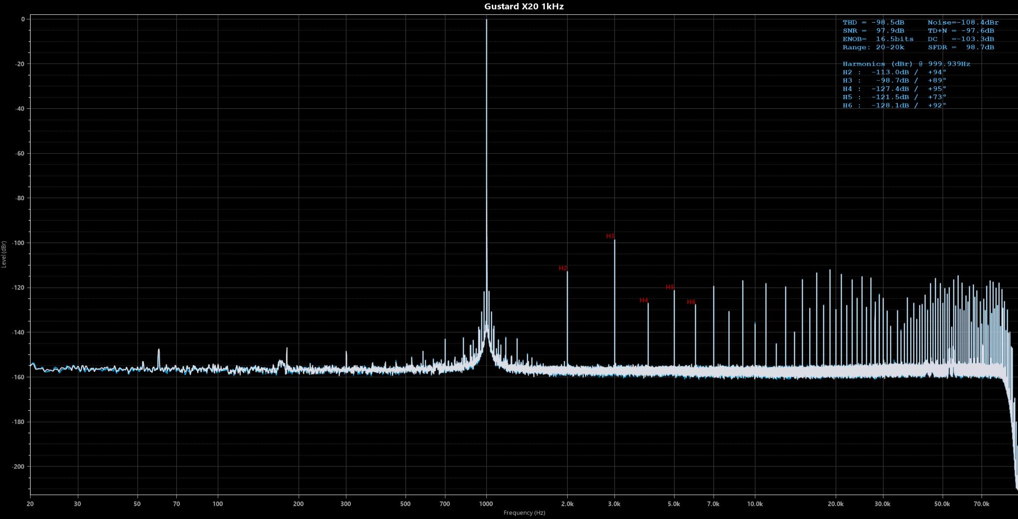
1kHz FFT:
Multitone 32:
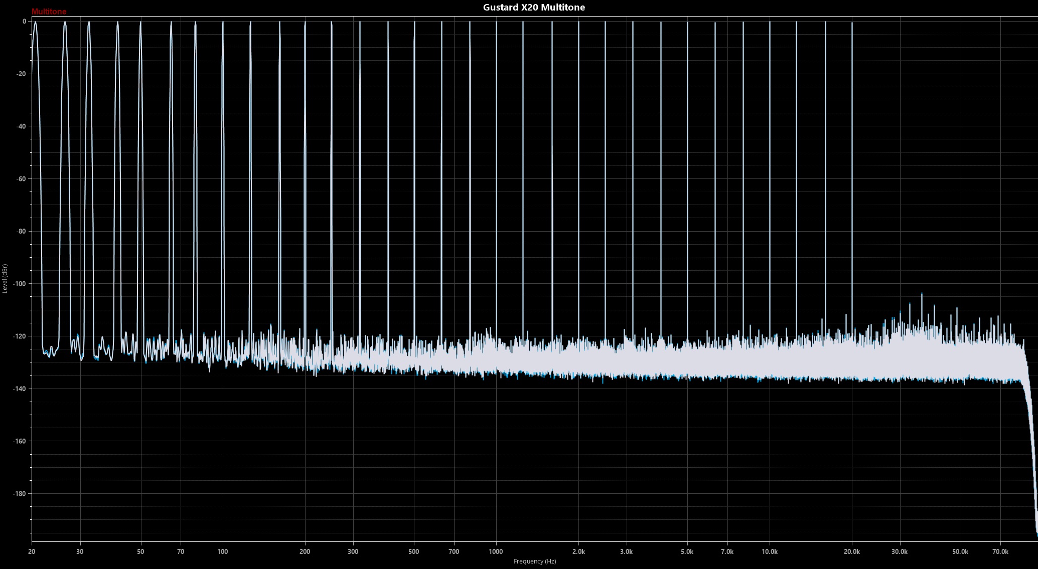
Look at those harmonics. Look at that third harmonic! That skirt! Yikes! Well, I say yikes, but this is a 2014 product. $600-ish 2014 USD would get you a DAC with ~100-105dB TD+N (again, my measurements always show 6-8dB worse than Amir's) with XLR, RCA, 32-bit volume control, LVDS I2S, AES, Optical, RCA SPDIF and even a BNS SPDIF connection. All in a sturdy brushed aluminum housing holding two rather large toroids complete with deparate PCBs for each part of the functionality, etcetera etcetera. But times have changed. Times have changed a lot.
The advent of cheaper silicon processes allowed more computing power to be shoved into chips. Process nodes shrank, LDO's got quieter, and that MCU which previously served as a display host and to set 1-8 registers is now responsible for 60+. There's onboard reclocking which is actually usable, and setting a precise oscillator right next to the DAC is now the de-facto standard. Onboard CLPDs for kitter control are now common right before the DAC chips in dual systems. Gustard, however, has always taken things a little too far. They tried to share a 100MHz clock from the digital board which was used to click the first (yes, there are two) CLPD which re-transmits all the input signals. This clock is shared across a coax cable and towers from the input board to the DAC board. It worked fine, and I think it is about the best execution of a terrible idea that can be had. But the execution still does not help the fact that the idea is terrible.
The Head-Fi thread has some great photos and has an occasional technical post but is mostly about cotton insulated OFC wires, stickers to go on top of capacitors, 'special' cotton wires for coax, etc. Nothing against those guys. They did properly identify some actual deficiencies in implementation, but then got absorbed in fixes involving a lot of marketing with nothing but subjective listening 'experiences' to guide them. Their heart is in the right place, but they may not have much interest in physics and math.
Output is handled in three stages:
- I/V happens across four AD4898-1 opamps. Feedback and filter components are all 1206 sized SMDs of proper selection. Power conditioning is handled by WIMA film capacitors on each rail.
- Differential matching is handled by a following OPA1632, one per channel. One side is dedicated to the 'hot' and the other to the 'cold'. The feedback network sets this to 2/3rd gain. (2390-Ohm input path, 1590-Ohm feedback path)
- Finally there is a discrete buffer. I have completely traced out one side of one channel. They are identical in construction for all four buffer circuits. If somebody wants to SPICE the circuit, I would be more than happy to see what it looks like. I am very curious if this buffer network could be better handled by a single opamp per 'layout' (four total opamps).
Here is one photo shamelessly taken from that same thread to illustrate the guts. I'm not sure if you can buy something with that many discrete components for the same number of inflation-adjusted dollars.
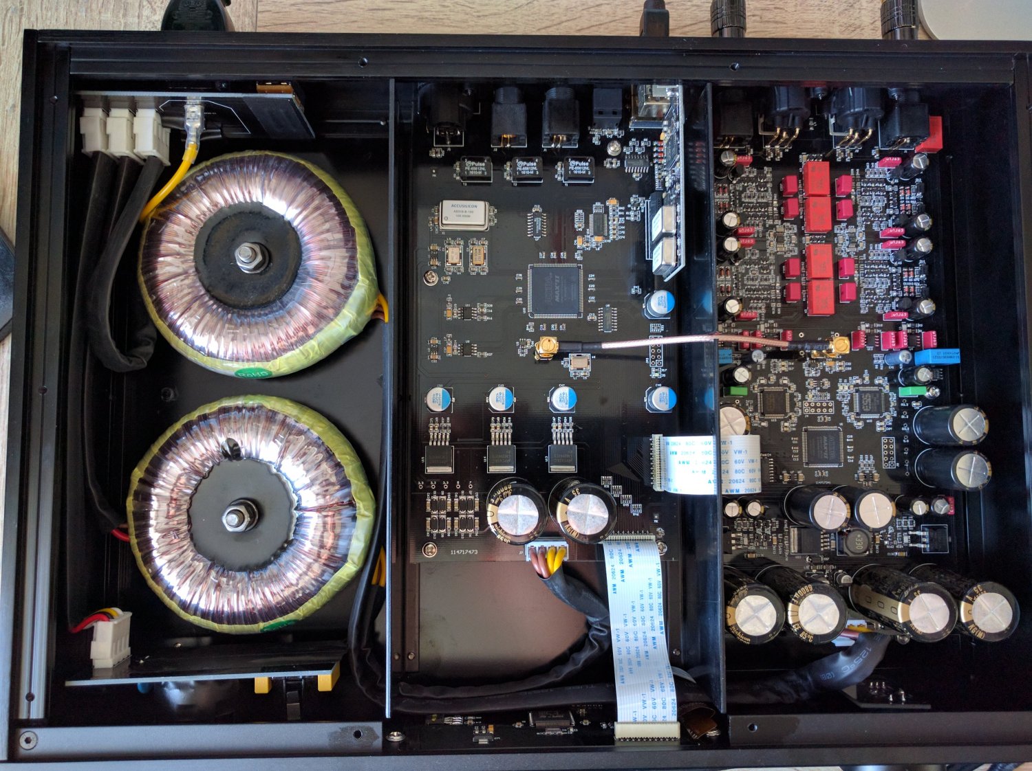
Performance aside, the symmetry and layout are very visually appealing. It's a good looking unit, even if I have very mixed feelings about a discrete buffer stage. I personally believe that a well-executed opamp stack will outperform it, but the X26Pro, the X16, the X18 all present compelling arguments. ESS has been very generous in making the 9018, 9028, and 9038 all identical in pinout (for the pro versions).
Anyway, the question I find myself asking, well.... myself; is this: Why spend the effort and capital to try and put two 9038Pros in this old, heavy, power-inefficient dinosaur?
The answer is simple and consists of two parts.
1. Why not?
2. Because I was offered two virgin 9038Pros for $30 USD. In late 2022.
3. (Bonus) Because deep down there might be a little masochism in me.
So let's start off with the challenges. First off, this is a terrible idea. Not just a terrible idea but an exclusively terrible idea. Maybe it is alright if you are a Buffalo III DAC owner but for anybody with a less modular PCB it's really just.... not worth it.
- 100dB TD+N is honestly going to be audibly transparent for the vast majority of real life situations.
- The 9038 is a HUNGRY chip. Each chip realistically needs bare minimum 300mA clean for AVCC and another 300mA for VDD. In dual mono, the VDD requirement goes from 1.2V to 1.3V just to allow more wattage. The ~130mA current requirement in the datasheet is with a 40MHz crystal and a 48kHz sample rate. Jump to 100MHz clock and 384kHz sample rate and you really want 500mA for each chip. From a power perspective, the 9038Pro was a massive step backward from the 9028Pro. In DimDim's excellent post about 9028Pro power draw we get to see the power requirement scaling. He is driving with a 100MHz oscillator. At 352.8kHz he was drawing 200mA on the core compared to the rated.... 82mA. Considering the 9038 has a good 50% higher draw we could easily see 300-350mA per chip at 384kHz, let alone 768kHz or DSD512+.
- Heat. Ever seen a naked 9038Pro without a heatsink run anywhere near full potential? It has an epad, which the 9018 never had, but it also always seems to sport a heatsink. The X20 has no ability to host any sort of epad nor real bottom dissipation. I have an idea here which I can discuss later.
- Output current. The 9038 has a ton of it. It has more output current than any SOIC opamp wants once you parallel four channels per opamp. It needs to take ~66-70mA in the I/V stage. Using traditional bipolar opamps is almost impossible without crippling the chip's capabilities. I believe this is why Gustard used a 'hybrid' opamp/discrete I/V on the dual 9038Pro X26Pro.
Let's look at the boards and strategize.
On the digital side I have removed the PCIE slot so I can wire USB I2S directly to the board. More importantly than that, I traced back the I2C pins to the onboard STM32. DimDim has an Arduino controller for the 90X8Pro based on a Due. I'm hoping with STMDuino I can port it over for the onboard STM32F407 chip controlling the Gustard display (512kb memory) and employ a J-link to flash it. I need to do alittle hell of a lot more research and work there. Firmware is where many of my projects get stuck. If anybody wants to help (out of curiosity/solidarity, or some other non-monetary motive) decompile a Gustard dump so we can modify for the register controls; or wishes to help port DimDim's Arduino code to STM34F407 I would offer my heartfelt gratitude. I can disassemble the front panel and reverse engineer the physical circuitry.
Supplying the beasts. Let's take stock of what we have. At the bottom of the photo is a set of test points. Unmarked is audio ground. The X20 does not utilize chassis ground as audio ground on the DAC board. There is no continuity between the mounting hole plates and the ground test point. -V and +V are the 15V rails rectified from the primary 50VA toroid. The digital board uses a separate 9V toroid. '5.0' is the basic digital board carrier voltage distributed to all the various LDOs. It can be checked next. Just to the right of that is 'O3.3' which is derived from the two LDOs next to the crystal socket. To the right of that point is 'D1.2' which is our digital core voltage, and next to that is 'R3.3" which is the LDO handling the right channel's AVCC. There is a corresponding 'D1.2' and 'L3.3' lext to the left channel's DAC chip. While AVCC is handled on a per-chip basis, the 1.2VDD is shared and both test points are directly coupled.
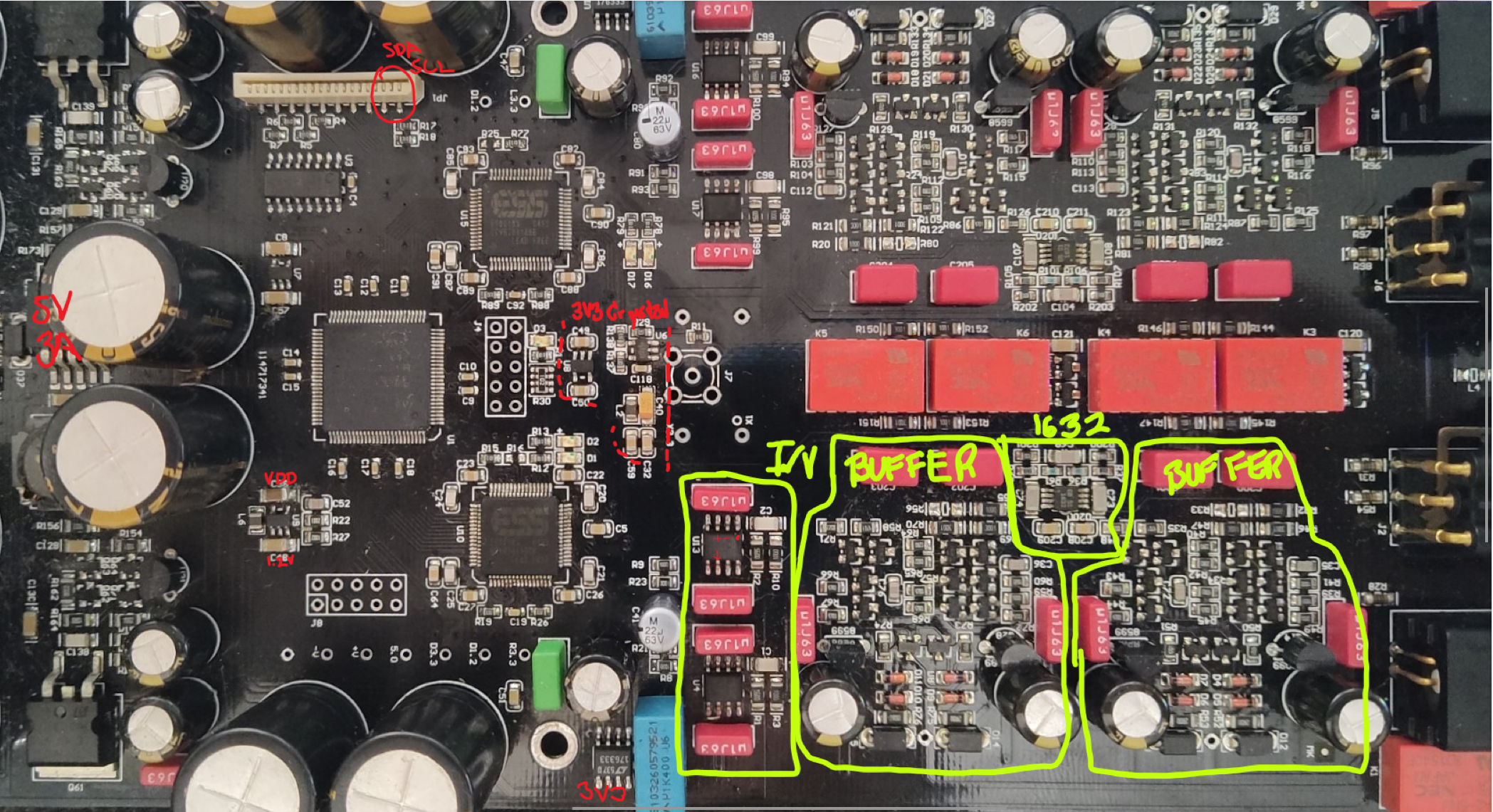
Starting from the front where the power comes in we set a rectumfried +15V and -15V from the toroid which is then passed at 30V through an LM2956. Each 15V leg is preserved for opamp rail usage. I tried to find LDOs in similar lead count with higher current and/or lower noise but it looks like that might be the only thing which will fit there. The LM2596 gives us the 5V and corresponds with test point '5.0.' The 5V is what is shared between the 3V3 LDOs and the 1V2 LDO. We have a significant +/- 15V budget to waste on opamp power and discrete buffer components but realistically about 12 clean watts or less to power both 9038Pros, the CPLD, and oscillator. IF we can keep each 9038 under 4-5W draw then everything should be gravy.
Coming off the 5V we see two SOT-23 LDOs to the right. The top is for the CPLD and features less filtering. The bottom is our 1.2V VDD for both DAC chips. For a dual mono 9038, this will need to be bumped to 1.3V. Remember how I Said the power requirements were kind of batty? Let's compare generations.

The 9028Pro is just a 9018s with updated digital core. We can see the input efficiency improvement with less than half power usage in the input O/S filter, jitter reduction circuitry, and DPLL/ channel mapping sections with increasing complexity each generation. Perhaps there was a process node shrink to a smaller die transistor size. The actual conversion cores though are a whole different beast. They hunger. The cores stalk the confines of their silicon home; looking for flowing electrons. They wait, patiently, for their prey to become available in great number. Finally they strike, quickly and viciously, howling and reveling in great charge lust; their writhing and machinations elevating temperatures to a level threatening their own existence.
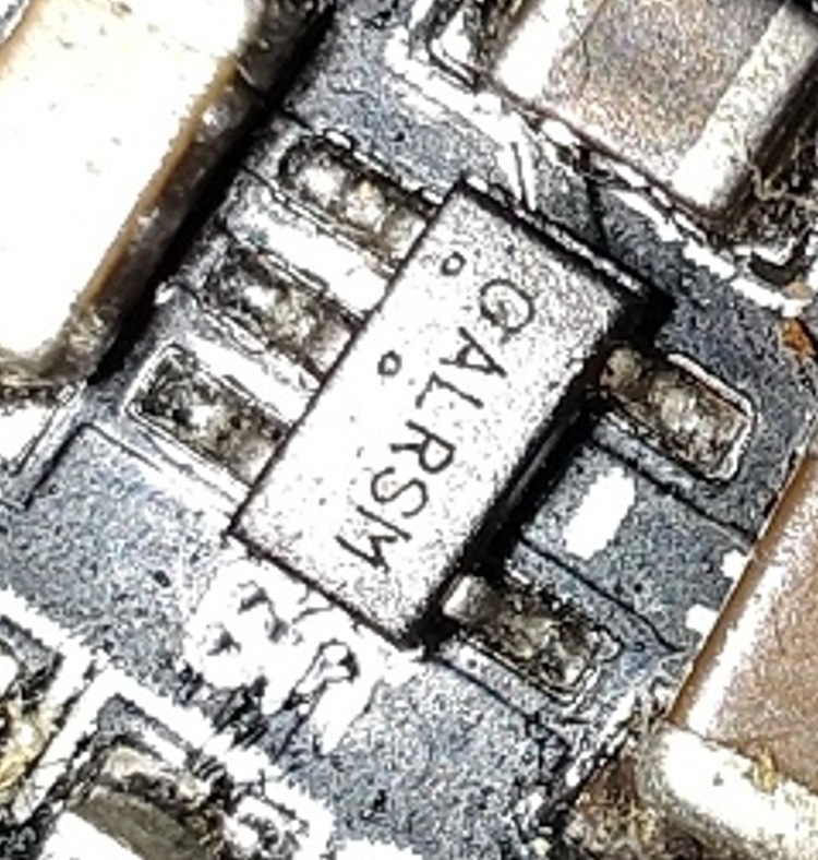
I could not find the make/model of the 1.2V regulator. The two dots are very similar to Richtek (usually noisy) but the 6-character code in a non-matrix laser marking indicates maybe Analog, Onsemi, or TI?
PLAN: LT3045-1A0G Ultra Low Noise LDO Voltage Regulator (1A) or TWO Twisted Pear Trident 1.3V (600mA per) (but that thing is massive and costly).
The 3V3 is provided by one LT1763 per chip. The LT1763 was never a bad chip, but the regs available today are far superior. It is specced at 20uV/rtHz which is pretty poor by the standards of the TPS7AXX series and LT3045. These have a WIMA MKP on the feed side and a SILMIC II on the load side. Some people complain about the SILMIC II in a power application. I honestly don;t think it would make much difference. In fact, a purpose-built power supply cap might be better than some fancy-schmantzy audio bull. From ELNA's prodyuct description: "Elna RFS (SILMIC II) Miniature High-Grade Capacitors for Audio use silk fibers for foil separation instead of paper. By using silk fibers and the fiber's pliability, the RFS (SILMIC II) Series offer high-grade superior acoustic sound for audio design. The RFS Capacitors can be used to relieve the music's harmonic vibration, increase the purity of the sound at high frequency, decrease muddy sound at the middle frequency, and increase high energy bass sound at low frequency."
Yeah.... that is all definitely happening from a power filtering electrolytic.....
Anyway, since I will likely be ordering from LDOVR (unless anybody else has a great regulator source with measured results) I can say that for now...
PLAN: Replace with 3.3v LT3045-78XXG Ultra Low Noise LDO Voltage Regulator.
The oscillator LDO is also probably equally noisy. For initial testing, I will be using the 100MHz oscillator stolen from an old SMSL M8. The future holds a different oscillator. Perhaps a Crystek CCPD-575X (+-20ppm / -90dBc/Hz ), or maybe SiTime 5359 (+-0.05ppm / -89dBc/Hz). I think these may pair nicely with a Ti TPS7A2033, as the PSRR vs Frequency and IOut graphs look promising, even if it has 7uVrms noise.
Cooling Tempers.
With 1.2/3V and 3.3V loosely addressed, we can talk about heat. There are not many options here. 9028 and 9038 can use epad to help address the issue, but that is a no-go here. Since the board was designed for 9018s with no epad, we can see a myriad of traces flowing under and around the chips on the bottom layer.
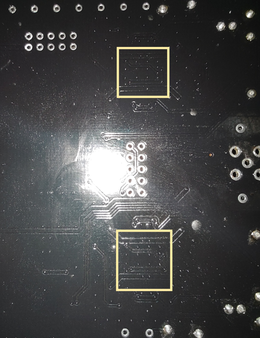
We do see a very thorough tie-in of grounding planes.
PLAN: I am thinking I might be able to mill a chunk of aluminum which is located by the chassis stand-offs. That piece would fill the gap between the chassis bottom plate (with some thermal goop) and the bottom of the PCB with two raised squares beneath each chip. Atop each of these squares could sit a non-conductive thermal pad. This would allow heat to transfer through the bottom of the chips into the huge thermal mass of the aluminum block and then into the casement itself. Some simple thermal adhesive sinks could ride on top of each device, or I could mill a larger sink for reliefs on the bottom for passive components and affix it with some thermal adhesive tape. This would give more thermal mass and more dissipation area at the cost of difficult removal in the future.
Now we can move on past the DAC chips themselves.
The Output.
The 9038 has a huge amount of current output. Parallel four channels per XLR hot/cold and you have a current supply that no SOIC-packaged opamp can handle and still produce decent TD+N when four channels are aparalleled. Other manufacturers have worked around this with hybrid I/V stages, multiple OPA1612's handling two channels each, and various other methods. Since I am working with a prebuilt PCB (and the wrong one for the real job) these were options which were unavailable to me.
Enter OPA1622. Wow! What a beast. 145mA current handling capability (even assuming that is for 2x opamps that is still 70+mA per opamp) with a THD and noise only bested by the OPA1611 and OPA1612. The AD4898 and AD797 both edge it out but nothing even comes close to this balance of distortion, noise, and capability.
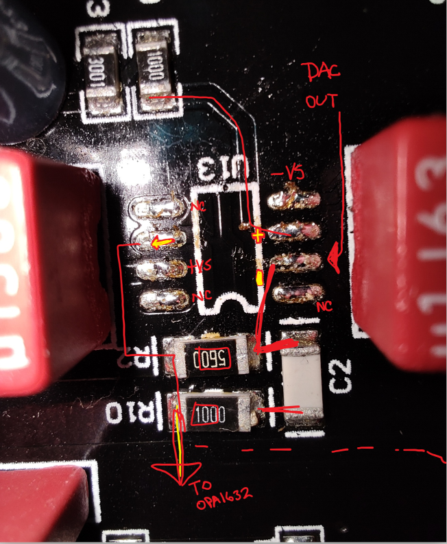
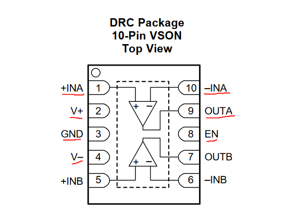
But... That layout. This is a dual opamp. The Gustard is set up for single opamps. This requires ground. The gustard has no ground pin on the original opamps. THe Gustard uses a SOIC-8 package. This is a VQFN. I/Os are nowhere close to the right size, shape, or location. What to do....
This is what we are working with:
This is where we want to be:
So I spun up EasyEDA and KiCAD. I was reminded why I do not use KiCAD when I tried to dynamically adjust trace paths and find something simple like an 0603 footprint. This is what I wound up with.
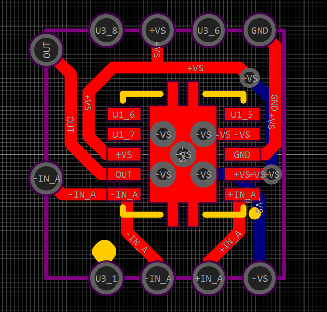
No orthogonal trace crossings. Layout only somewhat compromised on the +VS line. Feedback in and signal out will couple directly to the 1206 resistor next to the original opamp pads so as to try and keep feedback loop impedance low. Castellated holes with some wiggle room will secure the adapter board to the original pads. The signal ground plane exists right next to the pad two pins away from +VS. I can scrape away a tiny bit of solder mask and turn that NC into a GND. TI says that +VS can tie EN high. Total supply voltage is 30V and the part is rated for 36V. Ordered in 2Oz copper because they might get warm. Placed pad top and bottom which are tied to the OPA1622 pad. TI says to bring this to -VS. This allowed a sneaky bottom side entrance for the -VS line which simplified routing. I have never used a stencil before, but I ordered one this time. That entire PCB is 5.9mm wide. With a 560-Ohm feedback, the 9018's 15mA of current creates a 5.6Vpp signal. Since the 9038 will have ~66mA, the feedback must change. Looking at OPA1622 datasheet, we see the sweet spot is about 4-5Vrms:
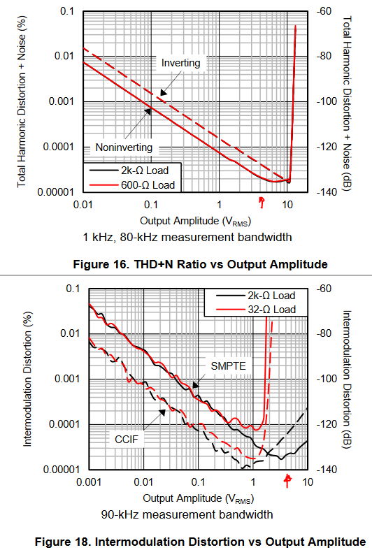
These measurements are max 2k-Ohm load. The OPA1632 will present a far higher load so the figures might scale a little better; but the OPA1622 has a max Vout of 14Vpp. If we shoot for 4Vrms that gives us 11.315Vpp. If we call it 171-Ohms then we get 11.286Vpp and 3.990Vrms. Multiply by two because each OPA1622 is only half of the OPA1632 input, pass that through the OPA1632's 2/3rds gain and get somewhere around 5.32Vrms fully differential output. This aligns very very very nicely with the OPA1632's lowest noise point.
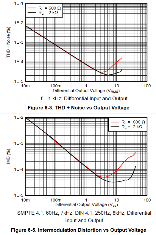
The 2nd stage I think can remain as-is. The 2nd stage will be difficult to improve. the OPA1632 has a TD+N of -132dB. I doubt those tightly coupled resistors and capacitors combined with that particular opamp will warrant any changes. Swapping to the 9038Pro might actually improve performance of the 2nd stage.
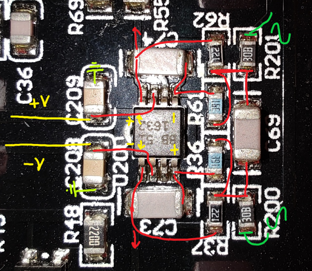
Now.... the output buffer. Oh my. This was both somewhat fun and very nightmarish to trace out.
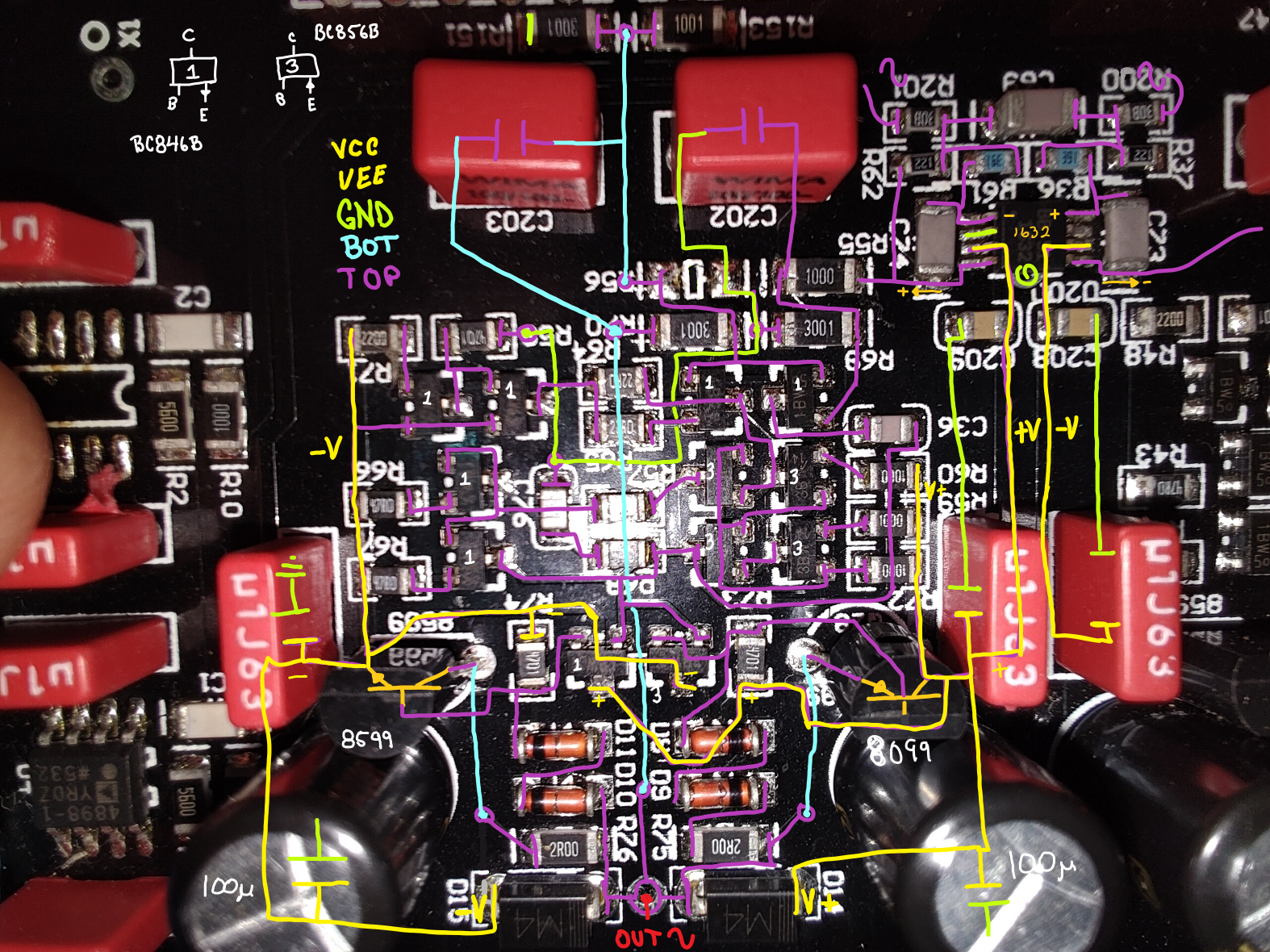
Everything here is rated for 25V+ so 3.2Vrms is not going to hurt it. The OPA1632 should see about a 5k differential load (measuring from cap to cap) which just puts it in its linear range. Specs show the as-delivered unit has a 4.6Vrms output on XLR. We know that the as-delivered I/V provides 8.4Vpp (560 ohms * 15mA). This is cut to 5.6Vpp (one leg) at the OPA1632 (8.4*2/3). That leaves us with 5.6Vpp for one side of the XLR. If we look at Vrms only for the hot, it should be 4.6Vrms/2 (hot and cold are out of phase, creating 2x differential from zero bias point) = 2.3Vrms = 6.506Vpp. 5.6Vpp = 1.98Vrms. So the buffer must be providing 1.1617x gain (6.506Vpp/5.6Vpp).
Ergo, if we feed 11.315Vpp from the I/V we will see 5.32Vrms full differential across the OPA1632. This would be 7.543Vpp per leg/buffer. Multiply that by the buffer gain 1.1617 and we have 8.7627Vpp per side of the XLR for a total output of 6.2Vrms. I believe the Gustard A18 had 6Vrms output, as did the X20Pro (ES9028Pro x2).
Again I must ask, why do I want to do this? I don't really know. But if I can get measurements as good or better than the 9018 after my butchering, I will consider it a success. Who knows, maybe I can even use those harmonic adjustment registers to cheat a bit.
Anyway, if you want to watch a disaster... stay tuned.
I was dead-set on improving a cheap 2x 9038Q2M DAC which measured just above 90dB TD+N. At one point, after frying the USB eeprom with a bad flash I broke out the Gustard and its accompanying Singxer SU-1 so I could use the Singxer to feed LVDS I2S into the cheapie. Once I had taken the cheap DAC from an okayish 91dB TD+N all the way to 108dB TD+N I was fairly satisfied. 108 may sound a little low but we are all spoiled. Everything I measure shows worse results than here so I am guessing it performs quite similarly to a Topping D10 Balanced.
Anyway, since the Gustard was sitting there on the floor I thought "why not?...." and that is how this all began. I failed to capture very detailed measurements because the numbers were disappointing enough I figured it would just go back into the closet.
1kHz FFT:
Multitone 32:
Look at those harmonics. Look at that third harmonic! That skirt! Yikes! Well, I say yikes, but this is a 2014 product. $600-ish 2014 USD would get you a DAC with ~100-105dB TD+N (again, my measurements always show 6-8dB worse than Amir's) with XLR, RCA, 32-bit volume control, LVDS I2S, AES, Optical, RCA SPDIF and even a BNS SPDIF connection. All in a sturdy brushed aluminum housing holding two rather large toroids complete with deparate PCBs for each part of the functionality, etcetera etcetera. But times have changed. Times have changed a lot.
The advent of cheaper silicon processes allowed more computing power to be shoved into chips. Process nodes shrank, LDO's got quieter, and that MCU which previously served as a display host and to set 1-8 registers is now responsible for 60+. There's onboard reclocking which is actually usable, and setting a precise oscillator right next to the DAC is now the de-facto standard. Onboard CLPDs for kitter control are now common right before the DAC chips in dual systems. Gustard, however, has always taken things a little too far. They tried to share a 100MHz clock from the digital board which was used to click the first (yes, there are two) CLPD which re-transmits all the input signals. This clock is shared across a coax cable and towers from the input board to the DAC board. It worked fine, and I think it is about the best execution of a terrible idea that can be had. But the execution still does not help the fact that the idea is terrible.
The Head-Fi thread has some great photos and has an occasional technical post but is mostly about cotton insulated OFC wires, stickers to go on top of capacitors, 'special' cotton wires for coax, etc. Nothing against those guys. They did properly identify some actual deficiencies in implementation, but then got absorbed in fixes involving a lot of marketing with nothing but subjective listening 'experiences' to guide them. Their heart is in the right place, but they may not have much interest in physics and math.
Output is handled in three stages:
- I/V happens across four AD4898-1 opamps. Feedback and filter components are all 1206 sized SMDs of proper selection. Power conditioning is handled by WIMA film capacitors on each rail.
- Differential matching is handled by a following OPA1632, one per channel. One side is dedicated to the 'hot' and the other to the 'cold'. The feedback network sets this to 2/3rd gain. (2390-Ohm input path, 1590-Ohm feedback path)
- Finally there is a discrete buffer. I have completely traced out one side of one channel. They are identical in construction for all four buffer circuits. If somebody wants to SPICE the circuit, I would be more than happy to see what it looks like. I am very curious if this buffer network could be better handled by a single opamp per 'layout' (four total opamps).
Here is one photo shamelessly taken from that same thread to illustrate the guts. I'm not sure if you can buy something with that many discrete components for the same number of inflation-adjusted dollars.
Performance aside, the symmetry and layout are very visually appealing. It's a good looking unit, even if I have very mixed feelings about a discrete buffer stage. I personally believe that a well-executed opamp stack will outperform it, but the X26Pro, the X16, the X18 all present compelling arguments. ESS has been very generous in making the 9018, 9028, and 9038 all identical in pinout (for the pro versions).
Anyway, the question I find myself asking, well.... myself; is this: Why spend the effort and capital to try and put two 9038Pros in this old, heavy, power-inefficient dinosaur?
The answer is simple and consists of two parts.
1. Why not?
2. Because I was offered two virgin 9038Pros for $30 USD. In late 2022.
3. (Bonus) Because deep down there might be a little masochism in me.
So let's start off with the challenges. First off, this is a terrible idea. Not just a terrible idea but an exclusively terrible idea. Maybe it is alright if you are a Buffalo III DAC owner but for anybody with a less modular PCB it's really just.... not worth it.
- 100dB TD+N is honestly going to be audibly transparent for the vast majority of real life situations.
- The 9038 is a HUNGRY chip. Each chip realistically needs bare minimum 300mA clean for AVCC and another 300mA for VDD. In dual mono, the VDD requirement goes from 1.2V to 1.3V just to allow more wattage. The ~130mA current requirement in the datasheet is with a 40MHz crystal and a 48kHz sample rate. Jump to 100MHz clock and 384kHz sample rate and you really want 500mA for each chip. From a power perspective, the 9038Pro was a massive step backward from the 9028Pro. In DimDim's excellent post about 9028Pro power draw we get to see the power requirement scaling. He is driving with a 100MHz oscillator. At 352.8kHz he was drawing 200mA on the core compared to the rated.... 82mA. Considering the 9038 has a good 50% higher draw we could easily see 300-350mA per chip at 384kHz, let alone 768kHz or DSD512+.
- Heat. Ever seen a naked 9038Pro without a heatsink run anywhere near full potential? It has an epad, which the 9018 never had, but it also always seems to sport a heatsink. The X20 has no ability to host any sort of epad nor real bottom dissipation. I have an idea here which I can discuss later.
- Output current. The 9038 has a ton of it. It has more output current than any SOIC opamp wants once you parallel four channels per opamp. It needs to take ~66-70mA in the I/V stage. Using traditional bipolar opamps is almost impossible without crippling the chip's capabilities. I believe this is why Gustard used a 'hybrid' opamp/discrete I/V on the dual 9038Pro X26Pro.
Let's look at the boards and strategize.
On the digital side I have removed the PCIE slot so I can wire USB I2S directly to the board. More importantly than that, I traced back the I2C pins to the onboard STM32. DimDim has an Arduino controller for the 90X8Pro based on a Due. I'm hoping with STMDuino I can port it over for the onboard STM32F407 chip controlling the Gustard display (512kb memory) and employ a J-link to flash it. I need to do a
Supplying the beasts. Let's take stock of what we have. At the bottom of the photo is a set of test points. Unmarked is audio ground. The X20 does not utilize chassis ground as audio ground on the DAC board. There is no continuity between the mounting hole plates and the ground test point. -V and +V are the 15V rails rectified from the primary 50VA toroid. The digital board uses a separate 9V toroid. '5.0' is the basic digital board carrier voltage distributed to all the various LDOs. It can be checked next. Just to the right of that is 'O3.3' which is derived from the two LDOs next to the crystal socket. To the right of that point is 'D1.2' which is our digital core voltage, and next to that is 'R3.3" which is the LDO handling the right channel's AVCC. There is a corresponding 'D1.2' and 'L3.3' lext to the left channel's DAC chip. While AVCC is handled on a per-chip basis, the 1.2VDD is shared and both test points are directly coupled.
Starting from the front where the power comes in we set a rectumfried +15V and -15V from the toroid which is then passed at 30V through an LM2956. Each 15V leg is preserved for opamp rail usage. I tried to find LDOs in similar lead count with higher current and/or lower noise but it looks like that might be the only thing which will fit there. The LM2596 gives us the 5V and corresponds with test point '5.0.' The 5V is what is shared between the 3V3 LDOs and the 1V2 LDO. We have a significant +/- 15V budget to waste on opamp power and discrete buffer components but realistically about 12 clean watts or less to power both 9038Pros, the CPLD, and oscillator. IF we can keep each 9038 under 4-5W draw then everything should be gravy.
Coming off the 5V we see two SOT-23 LDOs to the right. The top is for the CPLD and features less filtering. The bottom is our 1.2V VDD for both DAC chips. For a dual mono 9038, this will need to be bumped to 1.3V. Remember how I Said the power requirements were kind of batty? Let's compare generations.
The 9028Pro is just a 9018s with updated digital core. We can see the input efficiency improvement with less than half power usage in the input O/S filter, jitter reduction circuitry, and DPLL/ channel mapping sections with increasing complexity each generation. Perhaps there was a process node shrink to a smaller die transistor size. The actual conversion cores though are a whole different beast. They hunger. The cores stalk the confines of their silicon home; looking for flowing electrons. They wait, patiently, for their prey to become available in great number. Finally they strike, quickly and viciously, howling and reveling in great charge lust; their writhing and machinations elevating temperatures to a level threatening their own existence.
I could not find the make/model of the 1.2V regulator. The two dots are very similar to Richtek (usually noisy) but the 6-character code in a non-matrix laser marking indicates maybe Analog, Onsemi, or TI?
PLAN: LT3045-1A0G Ultra Low Noise LDO Voltage Regulator (1A) or TWO Twisted Pear Trident 1.3V (600mA per) (but that thing is massive and costly).
The 3V3 is provided by one LT1763 per chip. The LT1763 was never a bad chip, but the regs available today are far superior. It is specced at 20uV/rtHz which is pretty poor by the standards of the TPS7AXX series and LT3045. These have a WIMA MKP on the feed side and a SILMIC II on the load side. Some people complain about the SILMIC II in a power application. I honestly don;t think it would make much difference. In fact, a purpose-built power supply cap might be better than some fancy-schmantzy audio bull. From ELNA's prodyuct description: "Elna RFS (SILMIC II) Miniature High-Grade Capacitors for Audio use silk fibers for foil separation instead of paper. By using silk fibers and the fiber's pliability, the RFS (SILMIC II) Series offer high-grade superior acoustic sound for audio design. The RFS Capacitors can be used to relieve the music's harmonic vibration, increase the purity of the sound at high frequency, decrease muddy sound at the middle frequency, and increase high energy bass sound at low frequency."
Yeah.... that is all definitely happening from a power filtering electrolytic.....

Anyway, since I will likely be ordering from LDOVR (unless anybody else has a great regulator source with measured results) I can say that for now...
PLAN: Replace with 3.3v LT3045-78XXG Ultra Low Noise LDO Voltage Regulator.
The oscillator LDO is also probably equally noisy. For initial testing, I will be using the 100MHz oscillator stolen from an old SMSL M8. The future holds a different oscillator. Perhaps a Crystek CCPD-575X (+-20ppm / -90dBc/Hz ), or maybe SiTime 5359 (+-0.05ppm / -89dBc/Hz). I think these may pair nicely with a Ti TPS7A2033, as the PSRR vs Frequency and IOut graphs look promising, even if it has 7uVrms noise.
Cooling Tempers.
With 1.2/3V and 3.3V loosely addressed, we can talk about heat. There are not many options here. 9028 and 9038 can use epad to help address the issue, but that is a no-go here. Since the board was designed for 9018s with no epad, we can see a myriad of traces flowing under and around the chips on the bottom layer.
We do see a very thorough tie-in of grounding planes.
PLAN: I am thinking I might be able to mill a chunk of aluminum which is located by the chassis stand-offs. That piece would fill the gap between the chassis bottom plate (with some thermal goop) and the bottom of the PCB with two raised squares beneath each chip. Atop each of these squares could sit a non-conductive thermal pad. This would allow heat to transfer through the bottom of the chips into the huge thermal mass of the aluminum block and then into the casement itself. Some simple thermal adhesive sinks could ride on top of each device, or I could mill a larger sink for reliefs on the bottom for passive components and affix it with some thermal adhesive tape. This would give more thermal mass and more dissipation area at the cost of difficult removal in the future.
Now we can move on past the DAC chips themselves.
The Output.
The 9038 has a huge amount of current output. Parallel four channels per XLR hot/cold and you have a current supply that no SOIC-packaged opamp can handle and still produce decent TD+N when four channels are aparalleled. Other manufacturers have worked around this with hybrid I/V stages, multiple OPA1612's handling two channels each, and various other methods. Since I am working with a prebuilt PCB (and the wrong one for the real job) these were options which were unavailable to me.
Enter OPA1622. Wow! What a beast. 145mA current handling capability (even assuming that is for 2x opamps that is still 70+mA per opamp) with a THD and noise only bested by the OPA1611 and OPA1612. The AD4898 and AD797 both edge it out but nothing even comes close to this balance of distortion, noise, and capability.
But... That layout. This is a dual opamp. The Gustard is set up for single opamps. This requires ground. The gustard has no ground pin on the original opamps. THe Gustard uses a SOIC-8 package. This is a VQFN. I/Os are nowhere close to the right size, shape, or location. What to do....
This is what we are working with:
This is where we want to be:
So I spun up EasyEDA and KiCAD. I was reminded why I do not use KiCAD when I tried to dynamically adjust trace paths and find something simple like an 0603 footprint. This is what I wound up with.
No orthogonal trace crossings. Layout only somewhat compromised on the +VS line. Feedback in and signal out will couple directly to the 1206 resistor next to the original opamp pads so as to try and keep feedback loop impedance low. Castellated holes with some wiggle room will secure the adapter board to the original pads. The signal ground plane exists right next to the pad two pins away from +VS. I can scrape away a tiny bit of solder mask and turn that NC into a GND. TI says that +VS can tie EN high. Total supply voltage is 30V and the part is rated for 36V. Ordered in 2Oz copper because they might get warm. Placed pad top and bottom which are tied to the OPA1622 pad. TI says to bring this to -VS. This allowed a sneaky bottom side entrance for the -VS line which simplified routing. I have never used a stencil before, but I ordered one this time. That entire PCB is 5.9mm wide. With a 560-Ohm feedback, the 9018's 15mA of current creates a 5.6Vpp signal. Since the 9038 will have ~66mA, the feedback must change. Looking at OPA1622 datasheet, we see the sweet spot is about 4-5Vrms:
These measurements are max 2k-Ohm load. The OPA1632 will present a far higher load so the figures might scale a little better; but the OPA1622 has a max Vout of 14Vpp. If we shoot for 4Vrms that gives us 11.315Vpp. If we call it 171-Ohms then we get 11.286Vpp and 3.990Vrms. Multiply by two because each OPA1622 is only half of the OPA1632 input, pass that through the OPA1632's 2/3rds gain and get somewhere around 5.32Vrms fully differential output. This aligns very very very nicely with the OPA1632's lowest noise point.
The 2nd stage I think can remain as-is. The 2nd stage will be difficult to improve. the OPA1632 has a TD+N of -132dB. I doubt those tightly coupled resistors and capacitors combined with that particular opamp will warrant any changes. Swapping to the 9038Pro might actually improve performance of the 2nd stage.
Now.... the output buffer. Oh my. This was both somewhat fun and very nightmarish to trace out.
Everything here is rated for 25V+ so 3.2Vrms is not going to hurt it. The OPA1632 should see about a 5k differential load (measuring from cap to cap) which just puts it in its linear range. Specs show the as-delivered unit has a 4.6Vrms output on XLR. We know that the as-delivered I/V provides 8.4Vpp (560 ohms * 15mA). This is cut to 5.6Vpp (one leg) at the OPA1632 (8.4*2/3). That leaves us with 5.6Vpp for one side of the XLR. If we look at Vrms only for the hot, it should be 4.6Vrms/2 (hot and cold are out of phase, creating 2x differential from zero bias point) = 2.3Vrms = 6.506Vpp. 5.6Vpp = 1.98Vrms. So the buffer must be providing 1.1617x gain (6.506Vpp/5.6Vpp).
Ergo, if we feed 11.315Vpp from the I/V we will see 5.32Vrms full differential across the OPA1632. This would be 7.543Vpp per leg/buffer. Multiply that by the buffer gain 1.1617 and we have 8.7627Vpp per side of the XLR for a total output of 6.2Vrms. I believe the Gustard A18 had 6Vrms output, as did the X20Pro (ES9028Pro x2).
Again I must ask, why do I want to do this? I don't really know. But if I can get measurements as good or better than the 9018 after my butchering, I will consider it a success. Who knows, maybe I can even use those harmonic adjustment registers to cheat a bit.
Anyway, if you want to watch a disaster... stay tuned.
