• WANTED: Happy members who like to discuss audio and other topics related to our interest. Desire to learn and share knowledge of science required. There are many reviews of audio hardware and expert members to help answer your questions. Click here to have your audio equipment measured for free!

sabristol

Member
Forum Donor
Joined
Feb 23, 2021
Messages
52
Likes
111
This is a project I did last year - a mid 70s Luxman L-85v refurbishment with a re-engineered output stage.
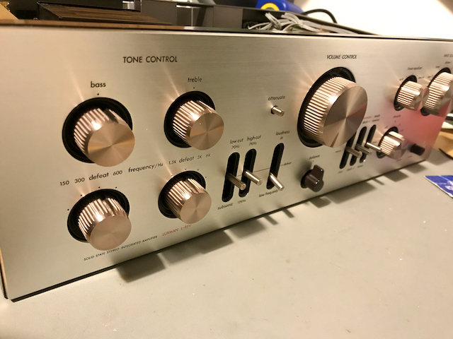
Luxman L-85v - 2.jpeg


The output stage PCBs were damaged in the early 1980s I've I had this amp kicking around since then. After 30 years, I eventually decided to try designing and building some replacements based on the Bob Cordell and Douglas Self books. After numerous attempts I ended up with:
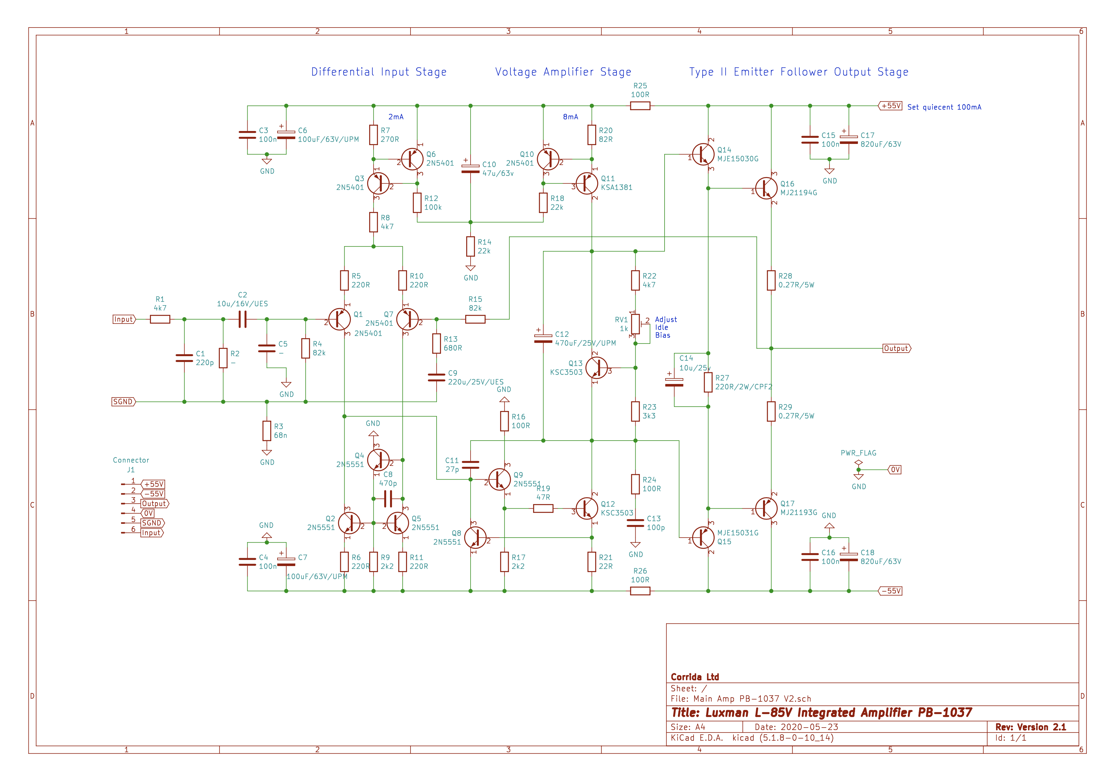
Screenshot 2021-02-23 at 11.49.23.png


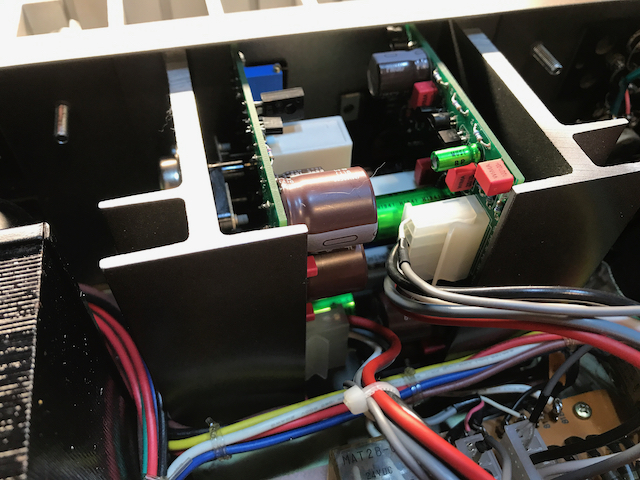
Here are the finished PCBs fitted:
Luxman L-85v - 9.jpeg


I thought this forum may be interested some of the tests I've put it through using the QuantAsylum QA-401 and QA451.

Frequency Response
Happy with the FR, although I could roll off the bottom end a little earlier.
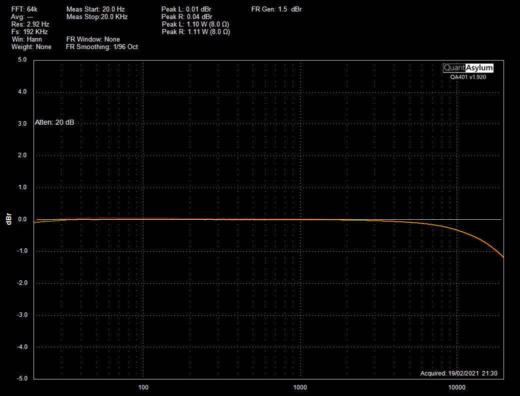
Luxman L85V - Frequency Response.png


THD v.s. Power
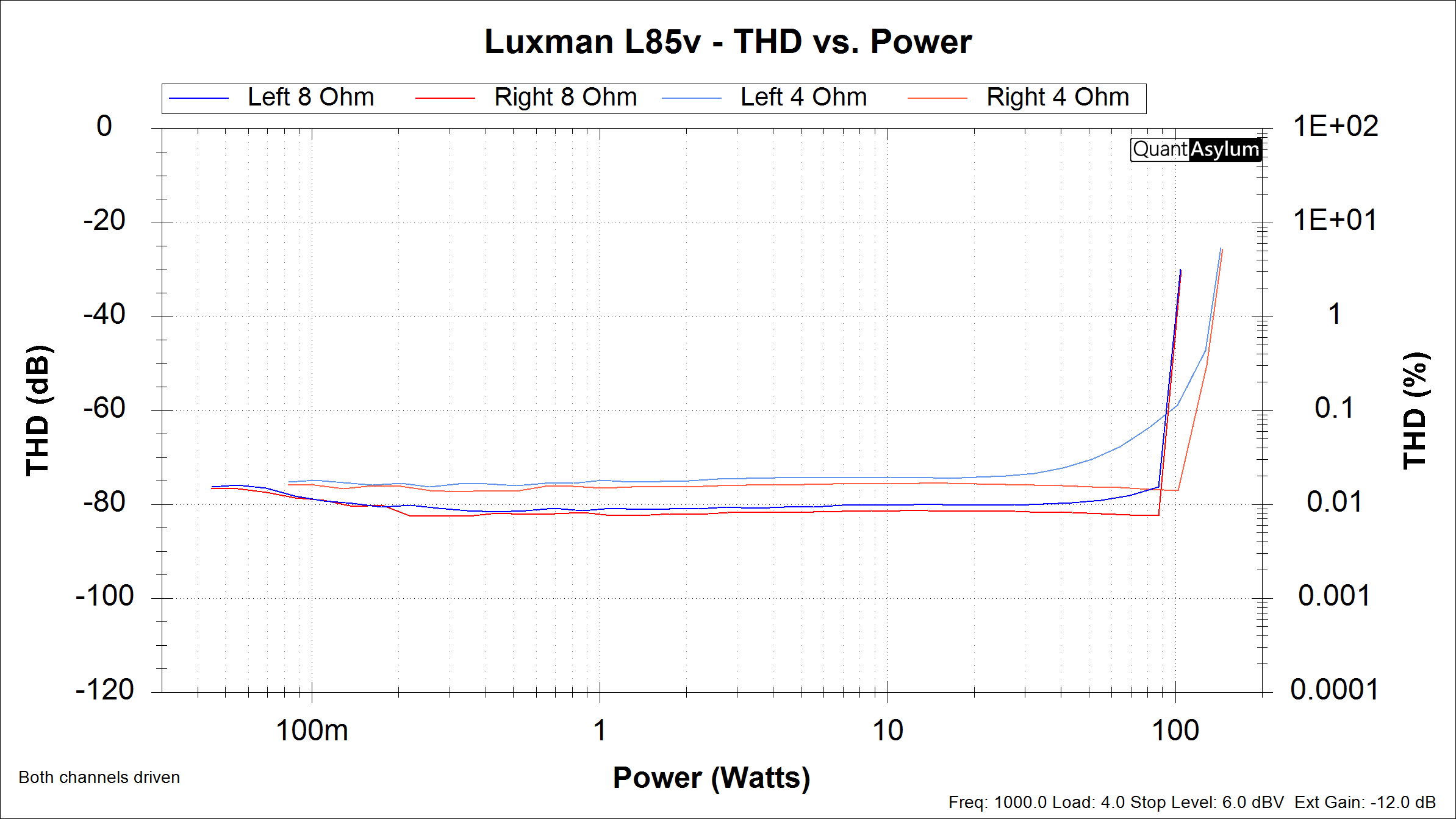
Happy with the results as better than OEM spec. It's odd that the left channel distorts earlier though and suspect this is due to output transistors. May change the left hand pair to see if that is the problem.
Luxman L85V - THD v.s. Power 4 & 8.png


Intermodulation Distortion
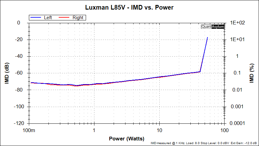
This is worse than the OEM spec, but suspect I'm not comparing like with like. The QA-401 uses 19k and 20k, whereas I expect the OEM test was at significantly lower.
Luxman L85V - IMD v.s. Power.png
IMD

Output Impedance
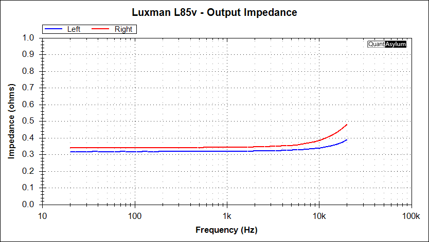
This seems a bit high as, if I understand this correctly it makes damping factor a paltry 8/0.35 = 23.
Luxman L85V - Output Impedance.png


My first post on here so I'd appreciate some constructive feedback!
 

Attachments

  • Luxman L-85v - 6.jpeg
    Luxman L-85v - 6.jpeg
    532 KB · Views: 828
I’ve been wanting a L-85V or L-80V for a bit now, but have been reluctant as I have no refurb skills.

Very very nice.
 
I’ve been wanting a L-85V or L-80V for a bit now, but have been reluctant as I have no refurb skills.

Very very nice.

Thanks.

I did the refurb originally with the intention of just selling it on as I have some Primare amps. I found I liked it so much though, I decided to keep it and even bought the matching Luxman T-88v tuner a couple of months ago off eBay. Due to COVID lockdown restrictions I've not been able to pick up and the seller won't post :-(

If this is a good forum (I'm new) I'll be posting the refurb of the tuner on here together with a few other hobby projects I've got on the go. Snippets here....
Cambridge - 1.jpeg

Hitachi - 1.jpeg
 
Your bias circuit is not failsafe. The ot should always go in the bottom leg.

Why 0.27 ohm emitter resistors instead of 0.22 ohm? What sort of bias level are you running?

Your output impedance may be mostly the output inductor and associated wiring. Distortion seems to be dominant 2nd and may be dominated by the preamp section, they don't tend to break any records. Usually -80 dB at rated power is about it, and that's actually good.

I would have been tempted to address the bizarro gain structure while you're at it. The tone control is a bizarre thing the likes of which I've only seen in '90s Yamaha AV receivers otherwise, not to mention it uses some known slightly problematic transistors (2SC1345).
 
Hi @AnalogSteph,

Thanks for the tip on the trim pot - good point, if it goes high we want no bias spread rather than maximum spread. The OEM design was topside too so may be one of the reasons why these amps go bang. They didn't appear to have any thermal bias compensation either whereas I've mounted Q13, Q14 and Q15 on the main heatsink.

I thought I was being brave choosing 0.27R instead of the 0.33R used in the OEM design. Should I lower it further? I'm running with 100mA quiescent which according to LTSpice gives me 87mA in Q16 and 7mA in Q14. I chose that from balancing optimum modelled distortion (which if I recollect correctly was minimal at 160mA) and real world idle temperature. The factory quiescent setting is 50mA.

I've not changed any of the output wiring or protection circuit which includes relays and inductors. Presumably the output impedance is essentially that network summed up with the emitter resistor and transistor Re?

For the preamp, I only recapped it rather than made any mods. I've not checked distortion of that separately so could be the source of some of the -80dB / 0.01% THD. As it was working, I hadn't noticed the two dodgy 2SC1345 Q101/102.

I guess it would be more informative to put the spectrum plot in such posts.

Many thanks for your feedback.
 
I thought I was being brave choosing 0.27R instead of the 0.33R used in the OEM design. Should I lower it further?
0.22 is sort of the standard these days for ~100wpc amplifiers. With your bias transistor being heatsink-mounted, that circuit should be quick and sensitive enough.
I'm running with 100mA quiescent which according to LTSpice gives me 87mA in Q16 and 7mA in Q14. I chose that from balancing optimum modelled distortion (which if I recollect correctly was minimal at 160mA) and real world idle temperature. The factory quiescent setting is 50mA.
Your bias seems a bit on the higher side. You may want to check what happens to bias dynamically when the amplifier is subjected to sine bursts. On a short time scale, thermal compensation can't do much, while output transistor junctions will heat up quickly. If bias is generous to begin with, the amplifier may temporarily enter overbiased terrain.

(You may want to consider mounting the bias spreader transistor as close to one of the output transistors as possible, e.g. on top of its tab or on opposing sides of the same heatsink. Output transistors with built-in bias diodes were a bit of a thing for a while but it seems they may not have worked quite as well as hoped.)
I've not changed any of the output wiring or protection circuit which includes relays and inductors. Presumably the output impedance is essentially that network summed up with the emitter resistor and transistor Re?
Not the latter two, which are inside the feedback loop. If those are still the original relays, I would suggest unsoldering and opening them to give the contacts a good cleaning. They should respond well to metal polish like Brasso or something on a cloth (contact cleaner should also work - if there is substantial arcing damage, the relay may have to be replaced; basically, by the time you have to resort to sandpaper it's toast). I would suggest making the relays as airtight as possible upon reassembly to minimize future tarnishing (maybe a thin line of silicone around the cover's base if that's the weak point, not so much that it couldn't be removed in the future).

The numerous switches in the signal path may, incidentally, appreciate similar treatment.
 
I like how you've used the original TO-3 transistor sockets and the placement of the two boards look lovely. What's the deal with that TO-220 that is almost touching the rear panel?

I've got a few L-81s at Dad's and an L-85V here partially restored for him.

The 2SC-1345s are the noisy Hitachi "tombstone" types IIRC.
1615268597525.png


If the leads are black (oxide) get them out fast.

Here's some pics of the original powerstage boards and the Lux L-85V I have here:

DSC_0468 (Medium).jpeg
DSC_0469 (Medium).jpeg
DSC_0474 (Medium).jpeg
DSC_0473 (Medium).jpeg
DSC_0483 (Medium).jpeg
 
The OEM design was topside too so may be one of the reasons why these amps go bang.

The amplifiers only go bang because of the epoxy 'blob' (spider's egg) STV diodes. (D501/502). They cause practically all the power stage problems in that series. The become flaky in these and all other brands that use them and should be replaced as a matter of course.

Other than that, they are rock solid designs.

The design was supposed to implement an STV (horseshoe style Sanken IIRC) compensation D503, but it was omitted and a 4.7k resistor put in its place.

1615272813013.png


Your output power at onset of clipping even in the good channels btw are actually in line or a little under a stock L-85V.
 
This is a project I did last year - a mid 70s Luxman L-85v refurbishment with a re-engineered output stage.
View attachment 114355

The output stage PCBs were damaged in the early 1980s I've I had this amp kicking around since then. After 30 years, I eventually decided to try designing and building some replacements based on the Bob Cordell and Douglas Self books. After numerous attempts I ended up with:
View attachment 114359

Here are the finished PCBs fitted:
View attachment 114360

I thought this forum may be interested some of the tests I've put it through using the QuantAsylum QA-401 and QA451.

Frequency Response
Happy with the FR, although I could roll off the bottom end a little earlier.
View attachment 114358

THD v.s. Power
Happy with the results as better than OEM spec. It's odd that the left channel distorts earlier though and suspect this is due to output transistors. May change the left hand pair to see if that is the problem.
View attachment 114361

Intermodulation Distortion
This is worse than the OEM spec, but suspect I'm not comparing like with like. The QA-401 uses 19k and 20k, whereas I expect the OEM test was at significantly lower.
View attachment 114362IMD

Output Impedance
This seems a bit high as, if I understand this correctly it makes damping factor a paltry 8/0.35 = 23.
View attachment 114372

My first post on here so I'd appreciate some constructive feedback!

Very nice job! I like the schematics and your choice of output devices MJL21194/93. They are very robust and still have reasonable hFE with Ic and frequency. If I built a new board I would probably use 2 pairs, to drive any load even 2 ohm.

There is a point in your measurements that surprises me. I would suppose that THD between 1W and 10W would be lower, near to -100dB, considering the circuit shown. Is there an explanation why it holds above -80dB? Would you be willing to post THD 1kHz distortion spectrum at 5W/4ohm?
It is also possible that the source of higher distortion are the other boards in the amp. Probably if you measured the power amp board in isolation it would have lower distortion. This is the reason why I do not like integrated amplifiers, the devil is usually hidden in preamp and EQ boards and wiring between the boards.
 
Last edited:
Your bias seems a bit on the higher side.

I do not think so, optimal bias of class AB is 20 - 25mV across Re (re distortion and distortion spectrum of the 2EF output stage). In case of Re = 0R27, it makes 74mA - 93mA.
 
Happy with the FR, although I could roll off the bottom end a little earlier.

Your bottom end rolloff is typical of the tested and reviewed FR plots of the L-85V. The top end however rolls off much more aggressively in your amplifier than both my experience with Lux L-xx amplifiers, and the UK technical review I have at hand. The L-85V review I have shows perhaps a maximum of -1dB at 40kHz and ruler flat to at least 30kHz. You are -1.25dB at 20kHz and only testing at 1W. Let's see what your PBW is.

The measured half power (40W/-3dB) bandwidth of the amplifier when new was 43kHz.

PS. What are the values of these components BTW? I presume your signal ground lift resistor is 68R.
1615277730284.png
 
Last edited:
Very nice job! I like the schematics and your choice of output devices MJL21194/93. They are very robust and still have reasonable hFE with Ic and frequency. If I built a new board I would probably use 2 pairs, to drive any load even 2 ohm.

There is a point in your measurements that surprises me. I would suppose that THD between 1W and 10W would be lower, near to -100dB, considering the circuit shown. Is there an explanation why it holds above -80dB? Would you be willing to post THD 1kHz distortion spectrum at 5W/4ohm?
It is also possible that the source of higher distortion are the other boards in the amp. Probably if you measured the power amp board in isolation it would have lower distortion. This is the reason why I do not like integrated amplifiers, the devil is usually hidden in preamp and EQ boards and wiring between the boards.
Thanks for the comments.

You're right, my test are done from line input so include the pre-amp/tone stage. I can easily make a harness for testing without though as I the wiring is socketed on the boards.

As soon as I get a chance I'll run another THD with a stepped range including 5W and post it.
 
I do not think so, optimal bias of class AB is 20 - 25mV across Re (re distortion and distortion spectrum of the 2EF output stage). In case of Re = 0R27, it makes 74mA - 93mA.

That is the same as I calculated using LTSpice using accurate transistor models: 87mA in Q16 and 7mA in Q14.
 
  • Like
Reactions: pma
The amplifiers only go bang because of the epoxy 'blob' (spider's egg) STV diodes. (D501/502). They cause practically all the power stage problems in that series. The become flaky in these and all other brands that use them and should be replaced as a matter of course.

Other than that, they are rock solid designs.

The design was supposed to implement an STV (horseshoe style Sanken IIRC) compensation D503, but it was omitted and a 4.7k resistor put in its place.

View attachment 117146

Your output power at onset of clipping even in the good channels btw are actually in line or a little under a stock L-85V.

I had clocked that modification to the bias spreader design. The service manual has D503 replaced with a 5k6 (mine had 4k7 factory fitted), and an extra 4R7 in the base of Q509. There are a couple errors on the schematic too: Z501 anode / C504 isn't connected to signal ground, rather 0V.

I haven't seen any actual test result for the L-85V, so other than the plots in the owners manual have no other reference point. Do you have some as I'd be interested to compare.
 
Thanks for the comments.

You're right, my test are done from line input so include the pre-amp/tone stage. I can easily make a harness for testing without though as I the wiring is socketed on the boards.

As soon as I get a chance I'll run another THD with a stepped range including 5W and post it.

I tried a brief simulation and the simulated 1kHz THD+N vs. power is somewhere between 0.001% and 0.01% (-100dB and -80dB), so probably the real world would not be better than -80dB. I have overlooked the high gain (82k/680R), so it is as it should be. Thanks for bringing this circuit into ASR!

Luxman_sch.png


Luxman_sim.png
 
Do you have some as I'd be interested to compare.

I have the original 1970s UK HiFi Choice extremely comprehensive and technical review of the L-85V and the L-80V, among many others. The only thing is, I have to carefully pull out the original pages to put on the scanner as the books are fragile.

I'll see what I can do.
 
I have the original 1970s UK HiFi Choice extremely comprehensive and technical review of the L-85V and the L-80V, among many others. The only thing is, I have to carefully pull out the original pages to put on the scanner as the books are fragile.

I'll see what I can do.

I would suggest just a photo. Both cameras and mobile phones are very good now and will give readable resolution.

P.S.: happy to see this technically oriented thread!!!!
 
I would suggest just a photo. Both cameras and mobile phones are very good now and will give readable resolution.

You know me, if I'm going to do it, I'll do it properly. The old B&K plotter images are small. ;)

I guess I'll have to finish restoring this L-85V here now, won't I, so we can compare...
 
Last edited:
I like how you've used the original TO-3 transistor sockets and the placement of the two boards look lovely. What's the deal with that TO-220 that is almost touching the rear panel?

I've got a few L-81s at Dad's and an L-85V here partially restored for him.

The 2SC-1345s are the noisy Hitachi "tombstone" types IIRC.
View attachment 117140

If the leads are black (oxide) get them out fast.

Here's some pics of the original powerstage boards and the Lux L-85V I have here:

View attachment 117141View attachment 117142View attachment 117143View attachment 117144View attachment 117145

As I'd increased the bias of this amp somewhat from the OEM spec, I decided to mount Q13 (bias spreader), Q14 and Q15 on the heatsink. This is the Kicad 3d.

Screenshot 2021-03-09 at 08.50.29.png


You look well organised. Good to see.

Have you changed the matched long tailed pair on your amp as mine were metal canned?

I see you've used Nichicon FG. I decided against that as there are some better suited for PSU decoupling and for the input and feedback coupling the books recommend bipolarised UES series. I'm sure it isn't measurable, even by Amir :)
 
Back
Top Bottom