Handling a complex load by power amplifiers
A power amplifier’s job is to supply a voltage to a loudspeaker and then to deliver whatever current the loudspeaker needs to move its voice coil, producing airwaves with a sound pressure level up to what is specified for the speaker and/or application. The output voltage multiplied with the resulting current constitutes the power that is delivered to the loudspeaker.
If we connect a resistor load to the amplifier’s output then things are simple; a resistor is a pure resistive and constant impedance. Between current through and voltage across the resistor there is zero phase shift, current and voltage have the same wave shape and resistor current can be directly calculated as I = V/R. Resistor power is then V*I or V^2/R. However, a loudspeaker is not a simple resistor, instead it can be seen as a coil with a resistance plus a resonant RLC circuit. This causes the loudspeaker’s ‘voltage to current’ transfer function to become complex, with the resulting impedance varying from the lowest ‘DC’ impedance to the impedance at the speaker’s resonance frequency, which can be much higher. The rated impedance listed in a loudspeaker’s data sheet is just an indication of the average.
More important is that a loudspeaker’s impedance is inductive below and capacitive above resonance, and inductive well above resonance, which means that voltage and current can be and are out of phase for most frequencies. Assuming we use a class A, B or AB amplifier, this poses a peak power issue. With a pure resistive load, at peak voltage the amplifier has to deliver also the peak current to the load. The voltage inside the amplifier is the difference between the amplifier’s power supply voltage and the output voltage. So, when delivering a peak voltage to the resistive load, even at a very high current the power dissipated inside the amplifier is limited, as it’s the product of a high current and a low internal voltage difference.
With a complex load, the phase between voltage and current changes with frequency. So there are frequencies where the current is out of phase with the voltage, asking the power amplifier to deliver the maximum current to the loudspeaker, while the voltage delivered to the loudspeaker is small. This means that the voltage difference inside the amplifier is much larger, compared to a pure resistive load. A high internal voltage difference multiplied by maximum current equals high power, so the power amplifier has to work much harder. This requires a lot from the output stage (the final power transistors) and the power supply, especially with high power loudspeakers with low impedances.
Testing power amplifiers with real loudspeakers instead of resistive dummy loads is difficult; needing to use loudspeaker arrays in isolated rooms or the use of large and expensive R-L-C dummy loads.
Apart from distortion - occurring when the power amplifier’s capabilities fall short of providing clean peak power - the main bottleneck is heat dissipation and even more the peak power in the output transistors. As we shall see later, transistor peak power can be much higher when the amplifier is feeding a complex load than when it is feeding a resistive load.
Characteristics of load used for tests
Two kinds of load were used for further testing, pure resistive load – power resistor 4.7ohm/200W, and a R-L-C dummy load that simulates impedance of the 7” SEAS woofer, the dummy load circuit schematics is shown below:
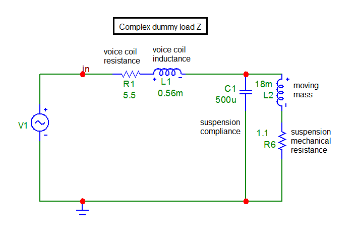
R1 and L1 are voice coil parameters, C1 and L2 and R6 represent cone parameters. The mechanical resistance is usually drawn in parallel with mass L2, but from a circuit view this has equivalent Q as my circuit and I have taken an advantage of the L2 intrinsic dc resistance to act as R6.
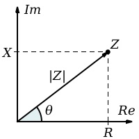
Though impedance Z of the pure resistive load equals to R and is a simple real number, impedance of the complex load Z is a complex number and must be represented in a 2-dimensional complex plane:
in Cartesian form:
Z = R + jX, where
R = Re(Z) … real part of Z, resistance
X = Im(Z) … imaginary part of Z, reactance
or in Polar form:
|Z| = sqrt(R^2 + X^2) … magnitude of impedance Z
Ø = arctan(X/R) … phase angle, represents phase angle between voltage and current
for more basic info on complex notation and complex impedance definition, please visit:

 en.wikipedia.org
Simulated dummy load impedance is in the further image:
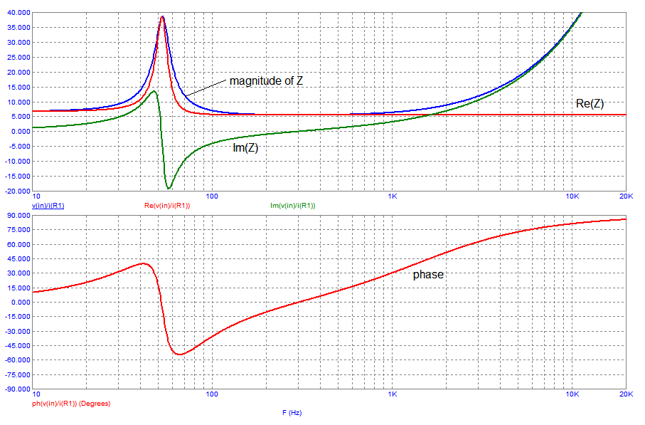
The plots show all the discussed impedance components, Re(Z), Im(Z), |Z| and Ø.
As a comparison there is another image with values of impedance magnitude and phase measured on the built dummy load.
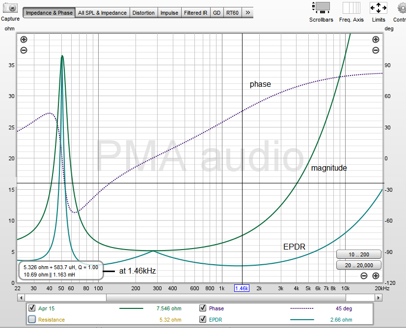
We can see very good conformance of measured values with simulated values. In this image we can also see EPDR plot, which means Equivalent Peak Dissipation Resistance, and is extremely important for evaluation of complex impedance impact to amplifier output stage, as we shall see later. EPDR plot shows an equivalent resistor value that would represent the same peak power loading as the complex load at the individual frequency. We can see that at 1460Hz, the EPDR = 2.66 ohm, though magnitude |Z| is seemingly benign 7.546 ohm with 45° phase angle.
Class AB amplifier driving resistive and complex load – comparison of peak power, simulation
First, let's assume a class B/AB amplifier driving a 4.7 ohm resistive load
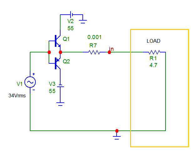
As an example, a pair of MJL3281/1302 “200W” transistors is driven from 34Vrms sine source and is supplied from 2 x 55Vdc power supply. The crucial parameter to be investigated is transistor's peak power. The allowed values of peak power are drawn in datasheets as a so called “Active Region Safe Operating Area” (SOA) and the plots show peak value of collector Ic current as a function of collector-emitter Vce voltage and time. The longer the time exposition to peak power, the lower allowed SOA.

So, we need to examine SOA in our circuit example for 4.7 ohm load. We need to see Ic as a function of Vce and compare it to SOA boundary from the datasheet. We shall use log scale for both Vce and Ic to make a comparison with the datasheet SOA plot feasible.
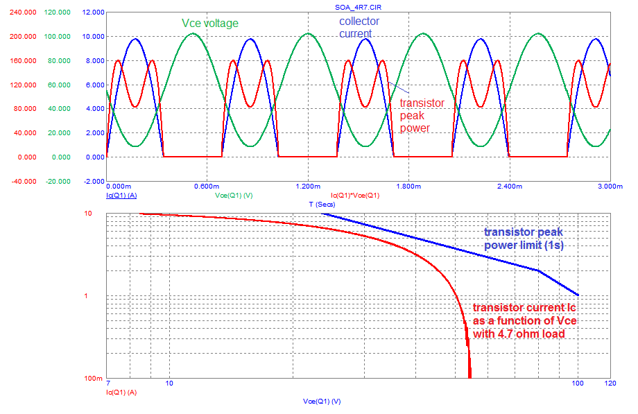
We can see that peak power is 160W and the Ic(Vce) red plot always remains below the 1s SOA blue boundary plot. So, with 1 pair of MJL3281/1302 200W/15A transistors we should be save with 4.7 ohm resistive load, when supply voltage is 2 x 55Vdc and output voltage is 34Vrms (load power 246W). Frequency of the sine source is unimportant in case we use the pure resistive load and power transistors are fast enough to handle the 20kHz bandwidth.
Now, let's move to the complex dummy load that simulates a single speaker, 7” woofer. This is the circuit for simulation
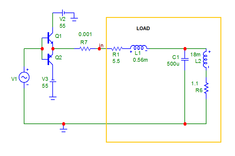
Please note that dc resistance of the dummy load is 6.6 ohm and thus is higher than the 4.7 ohm resistor resistance used in the previous SOA examination. The impedance plots of this load were shown here above.
The impedance plots of this complex load were shown above and we shall concentrate our examination efforts to the frequency where we have lowest EPDR at considerably high phase angle. Both our intuition, when reading the impedance and EPDR plots, and intensive simulation over wide range of frequencies confirm that the frequencies of concerns are near to 1460 Hz. At 1460 Hz, we have impedance magnitude |Z| = 7.546 ohm, phase angle Ø = +45°, but EPDR = 2.66 ohm! So the peak dissipation factor for output transistors equals to 2.66 ohm resistor, with the load that has 7.546 ohm impedance seen in a conventional way.
Let's start a simulation:
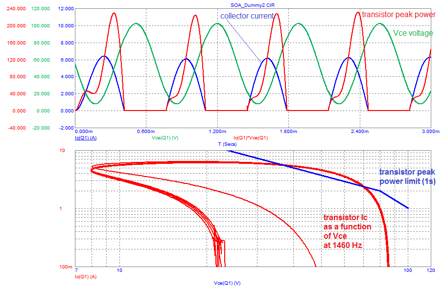
We can see that transistor peak stress values have changed significantly, compared to the 4.7 ohm resistor load. Vce(peak) = 102.2 V (same), Ic(peak) = 6.2A (much lower), but P(peak) = 231.3W – much higher than in case of 4.7 ohm load, when it was 160W. The key to this behaviour is a phase angle between load current I(load) and load voltage V(load), that results in different P = Vce*Ic instant power values than in case of a resistor load, where resistor current and voltage are in phase. The simulated circuit SOA is now exceeded, the Ic(Vce) red plot jumps above the SOA boundary blue plot. We would need to add one more pair of output transistors, in parallel with the existing pair, to keep the amplifier on a safe side of SOA, with this complex load.
Impact of complex load to distortion
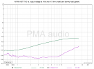
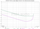
The impact of complex load impedance to amplifier distortion is not quite straightforward when we look at impedance magnitude and phase plots. Measurements of THD+N vs. frequency and THD+N vs. output voltage at 1kHz were done to illustrate it. The A250W4R class AB amplifier was used for these measurements.
THD+N vs. frequency at 7Vrms output voltage
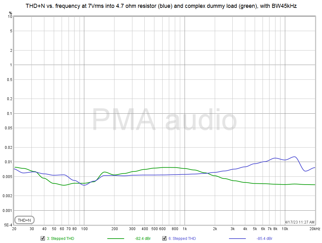
We can see that distortion with the complex load is lower except of the area between approx. 200Hz – 1700Hz. At 278Hz, the complex load impedance is purely resistive and equals to 5 ohm. Below 278Hz we can also see the capacitive part of impedance and above 278Hz starts inductive part of impedance. At 1700Hz, magnitude |Z| is 8.3 ohm, EPDR is 3.03 ohm and phase +49°. Above 1700Hz, distortion with complex load is lower than with the 4.7 ohm resistor, though phase is getting high up to +83°. At 1700Hz and above it, the complex impedance might be modelled by a series connection of 5.37 ohm resistor and 0.586 mH inductor. Quite predictable from the dummy load circuit schematics.
THD+N vs. output voltage at 1kHz
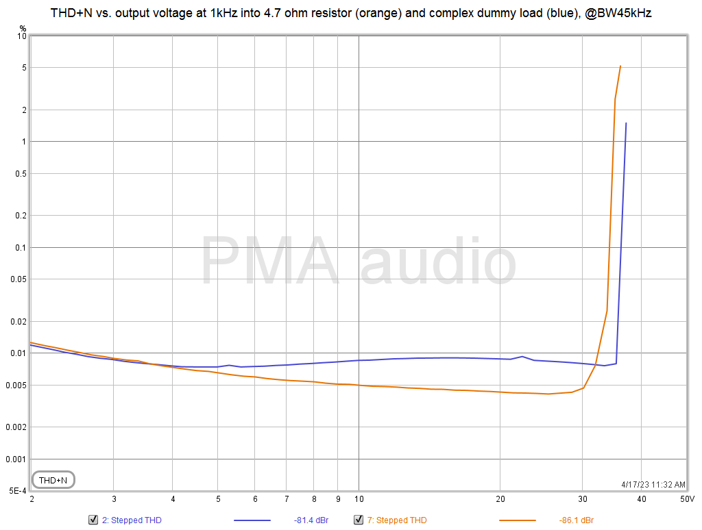
At 1kHz we have impedance magnitude |Z| = 6.336 ohm, phase = +34° and EPDR = 2.74 ohm. Compared to distortion with 4.7 ohm resistor, the distortion with complex impedance at 1kHz is higher.
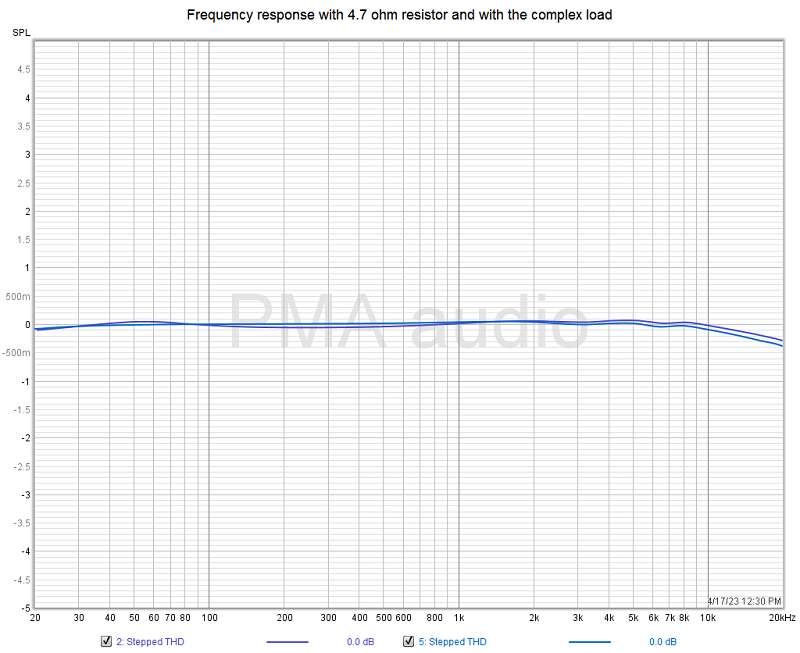
The impact of this complex load to frequency response of the amplifier used was negligible.
Conclusion
The simulations show high impact of complex loads to class AB amplifier peak power stress of the output transistors. This is in general valid for all kinds of linear amplifiers. The impact of complex impedances to amplifier distortion is not quite straightforward and may be only guessed from the impedance plots. What might be the issue from the point of view of peak power dissipation does not necessarily reflect in high distortion, in case that output devices are not destroyed.
In case of class D amplifiers, when the output transistors dissipate the power mostly during the switching transitions, it is impossible to draw any conclusions from the data I have posted here. Further investigation will be necessary.
Further reading:

 www.stereophile.com
__________________________________________________________________________________________________________________________________________
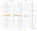
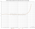
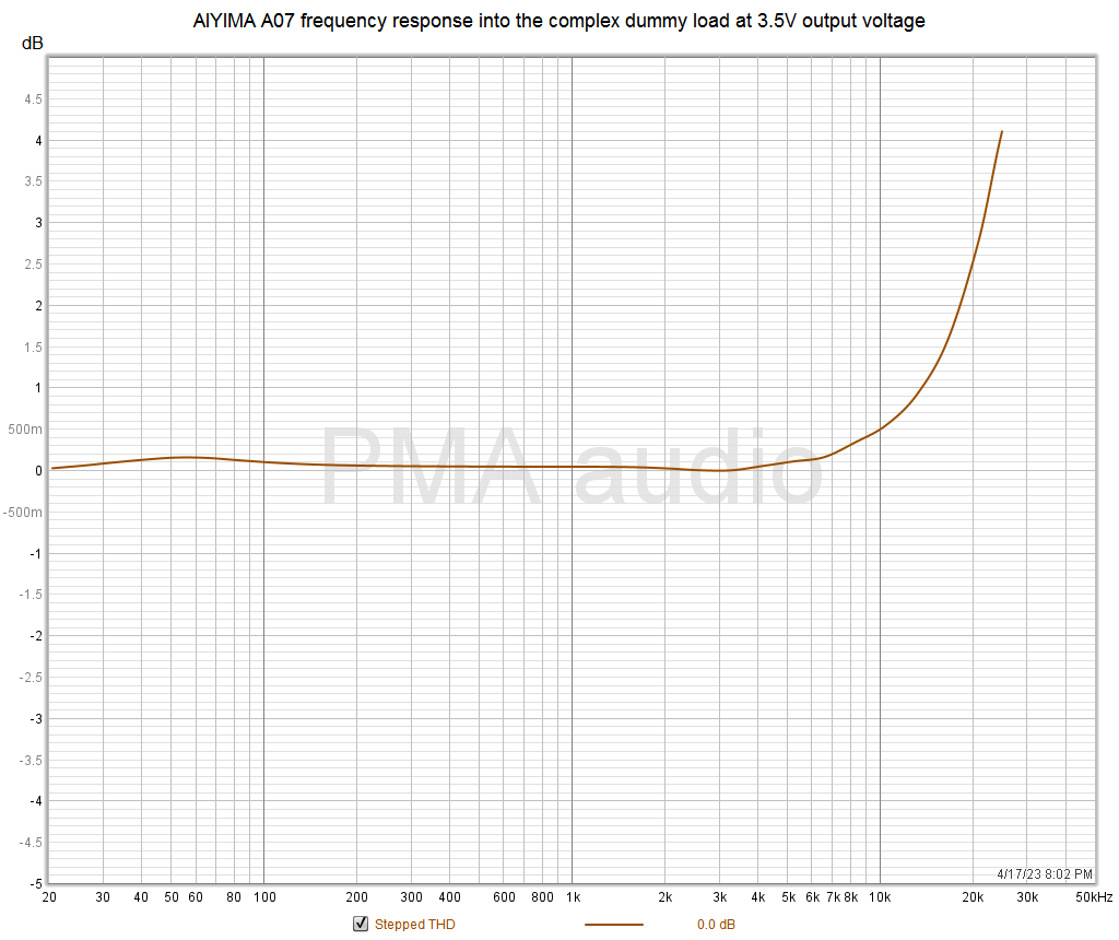
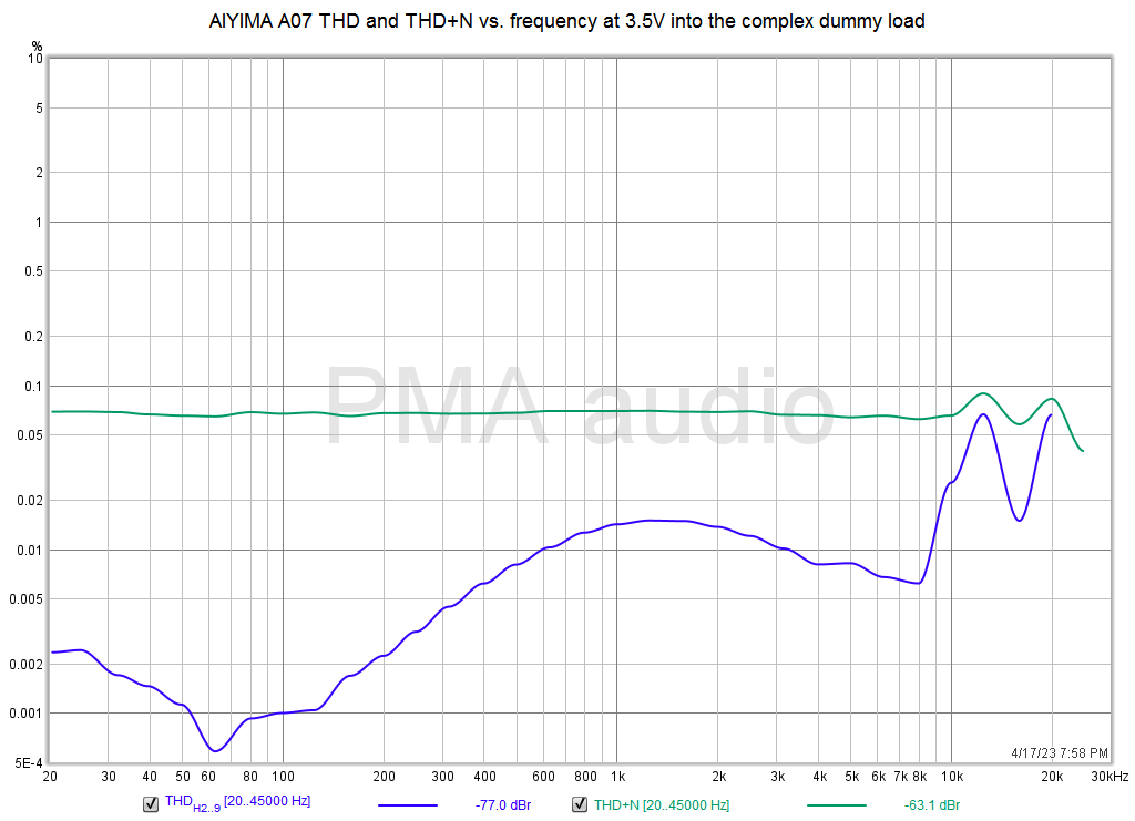
Several hours later - I have just started to test class D amplifiers with the complex load shown in this thread. First on the bench is AIYIMA A07 and the results are worse than I have expected. The amplifier is unable to handle frequency sweep from 20Hz to 30kHz even at low output voltage 3.5V. It is able to manage the stepped sine frequency test, however. Below are the results, frequency response and distortion vs. frequency. To drive a full range speaker with 1 driver, the amplifier would not be usable.


A power amplifier’s job is to supply a voltage to a loudspeaker and then to deliver whatever current the loudspeaker needs to move its voice coil, producing airwaves with a sound pressure level up to what is specified for the speaker and/or application. The output voltage multiplied with the resulting current constitutes the power that is delivered to the loudspeaker.
If we connect a resistor load to the amplifier’s output then things are simple; a resistor is a pure resistive and constant impedance. Between current through and voltage across the resistor there is zero phase shift, current and voltage have the same wave shape and resistor current can be directly calculated as I = V/R. Resistor power is then V*I or V^2/R. However, a loudspeaker is not a simple resistor, instead it can be seen as a coil with a resistance plus a resonant RLC circuit. This causes the loudspeaker’s ‘voltage to current’ transfer function to become complex, with the resulting impedance varying from the lowest ‘DC’ impedance to the impedance at the speaker’s resonance frequency, which can be much higher. The rated impedance listed in a loudspeaker’s data sheet is just an indication of the average.
More important is that a loudspeaker’s impedance is inductive below and capacitive above resonance, and inductive well above resonance, which means that voltage and current can be and are out of phase for most frequencies. Assuming we use a class A, B or AB amplifier, this poses a peak power issue. With a pure resistive load, at peak voltage the amplifier has to deliver also the peak current to the load. The voltage inside the amplifier is the difference between the amplifier’s power supply voltage and the output voltage. So, when delivering a peak voltage to the resistive load, even at a very high current the power dissipated inside the amplifier is limited, as it’s the product of a high current and a low internal voltage difference.
With a complex load, the phase between voltage and current changes with frequency. So there are frequencies where the current is out of phase with the voltage, asking the power amplifier to deliver the maximum current to the loudspeaker, while the voltage delivered to the loudspeaker is small. This means that the voltage difference inside the amplifier is much larger, compared to a pure resistive load. A high internal voltage difference multiplied by maximum current equals high power, so the power amplifier has to work much harder. This requires a lot from the output stage (the final power transistors) and the power supply, especially with high power loudspeakers with low impedances.
Testing power amplifiers with real loudspeakers instead of resistive dummy loads is difficult; needing to use loudspeaker arrays in isolated rooms or the use of large and expensive R-L-C dummy loads.
Apart from distortion - occurring when the power amplifier’s capabilities fall short of providing clean peak power - the main bottleneck is heat dissipation and even more the peak power in the output transistors. As we shall see later, transistor peak power can be much higher when the amplifier is feeding a complex load than when it is feeding a resistive load.
Characteristics of load used for tests
Two kinds of load were used for further testing, pure resistive load – power resistor 4.7ohm/200W, and a R-L-C dummy load that simulates impedance of the 7” SEAS woofer, the dummy load circuit schematics is shown below:
R1 and L1 are voice coil parameters, C1 and L2 and R6 represent cone parameters. The mechanical resistance is usually drawn in parallel with mass L2, but from a circuit view this has equivalent Q as my circuit and I have taken an advantage of the L2 intrinsic dc resistance to act as R6.
Though impedance Z of the pure resistive load equals to R and is a simple real number, impedance of the complex load Z is a complex number and must be represented in a 2-dimensional complex plane:
in Cartesian form:
Z = R + jX, where
R = Re(Z) … real part of Z, resistance
X = Im(Z) … imaginary part of Z, reactance
or in Polar form:
|Z| = sqrt(R^2 + X^2) … magnitude of impedance Z
Ø = arctan(X/R) … phase angle, represents phase angle between voltage and current
for more basic info on complex notation and complex impedance definition, please visit:

Electrical impedance - Wikipedia
Simulated dummy load impedance is in the further image:
The plots show all the discussed impedance components, Re(Z), Im(Z), |Z| and Ø.
As a comparison there is another image with values of impedance magnitude and phase measured on the built dummy load.
We can see very good conformance of measured values with simulated values. In this image we can also see EPDR plot, which means Equivalent Peak Dissipation Resistance, and is extremely important for evaluation of complex impedance impact to amplifier output stage, as we shall see later. EPDR plot shows an equivalent resistor value that would represent the same peak power loading as the complex load at the individual frequency. We can see that at 1460Hz, the EPDR = 2.66 ohm, though magnitude |Z| is seemingly benign 7.546 ohm with 45° phase angle.
Class AB amplifier driving resistive and complex load – comparison of peak power, simulation
First, let's assume a class B/AB amplifier driving a 4.7 ohm resistive load
As an example, a pair of MJL3281/1302 “200W” transistors is driven from 34Vrms sine source and is supplied from 2 x 55Vdc power supply. The crucial parameter to be investigated is transistor's peak power. The allowed values of peak power are drawn in datasheets as a so called “Active Region Safe Operating Area” (SOA) and the plots show peak value of collector Ic current as a function of collector-emitter Vce voltage and time. The longer the time exposition to peak power, the lower allowed SOA.
So, we need to examine SOA in our circuit example for 4.7 ohm load. We need to see Ic as a function of Vce and compare it to SOA boundary from the datasheet. We shall use log scale for both Vce and Ic to make a comparison with the datasheet SOA plot feasible.
We can see that peak power is 160W and the Ic(Vce) red plot always remains below the 1s SOA blue boundary plot. So, with 1 pair of MJL3281/1302 200W/15A transistors we should be save with 4.7 ohm resistive load, when supply voltage is 2 x 55Vdc and output voltage is 34Vrms (load power 246W). Frequency of the sine source is unimportant in case we use the pure resistive load and power transistors are fast enough to handle the 20kHz bandwidth.
Now, let's move to the complex dummy load that simulates a single speaker, 7” woofer. This is the circuit for simulation
Please note that dc resistance of the dummy load is 6.6 ohm and thus is higher than the 4.7 ohm resistor resistance used in the previous SOA examination. The impedance plots of this load were shown here above.
The impedance plots of this complex load were shown above and we shall concentrate our examination efforts to the frequency where we have lowest EPDR at considerably high phase angle. Both our intuition, when reading the impedance and EPDR plots, and intensive simulation over wide range of frequencies confirm that the frequencies of concerns are near to 1460 Hz. At 1460 Hz, we have impedance magnitude |Z| = 7.546 ohm, phase angle Ø = +45°, but EPDR = 2.66 ohm! So the peak dissipation factor for output transistors equals to 2.66 ohm resistor, with the load that has 7.546 ohm impedance seen in a conventional way.
Let's start a simulation:
We can see that transistor peak stress values have changed significantly, compared to the 4.7 ohm resistor load. Vce(peak) = 102.2 V (same), Ic(peak) = 6.2A (much lower), but P(peak) = 231.3W – much higher than in case of 4.7 ohm load, when it was 160W. The key to this behaviour is a phase angle between load current I(load) and load voltage V(load), that results in different P = Vce*Ic instant power values than in case of a resistor load, where resistor current and voltage are in phase. The simulated circuit SOA is now exceeded, the Ic(Vce) red plot jumps above the SOA boundary blue plot. We would need to add one more pair of output transistors, in parallel with the existing pair, to keep the amplifier on a safe side of SOA, with this complex load.
Impact of complex load to distortion
The impact of complex load impedance to amplifier distortion is not quite straightforward when we look at impedance magnitude and phase plots. Measurements of THD+N vs. frequency and THD+N vs. output voltage at 1kHz were done to illustrate it. The A250W4R class AB amplifier was used for these measurements.
THD+N vs. frequency at 7Vrms output voltage
We can see that distortion with the complex load is lower except of the area between approx. 200Hz – 1700Hz. At 278Hz, the complex load impedance is purely resistive and equals to 5 ohm. Below 278Hz we can also see the capacitive part of impedance and above 278Hz starts inductive part of impedance. At 1700Hz, magnitude |Z| is 8.3 ohm, EPDR is 3.03 ohm and phase +49°. Above 1700Hz, distortion with complex load is lower than with the 4.7 ohm resistor, though phase is getting high up to +83°. At 1700Hz and above it, the complex impedance might be modelled by a series connection of 5.37 ohm resistor and 0.586 mH inductor. Quite predictable from the dummy load circuit schematics.
THD+N vs. output voltage at 1kHz
At 1kHz we have impedance magnitude |Z| = 6.336 ohm, phase = +34° and EPDR = 2.74 ohm. Compared to distortion with 4.7 ohm resistor, the distortion with complex impedance at 1kHz is higher.
The impact of this complex load to frequency response of the amplifier used was negligible.
Conclusion
The simulations show high impact of complex loads to class AB amplifier peak power stress of the output transistors. This is in general valid for all kinds of linear amplifiers. The impact of complex impedances to amplifier distortion is not quite straightforward and may be only guessed from the impedance plots. What might be the issue from the point of view of peak power dissipation does not necessarily reflect in high distortion, in case that output devices are not destroyed.
In case of class D amplifiers, when the output transistors dissipate the power mostly during the switching transitions, it is impossible to draw any conclusions from the data I have posted here. Further investigation will be necessary.
Further reading:

Heavy Load: How Loudspeakers Torture Amplifiers
Why, in loudspeaker reviews, is impedance measured (assuming that the magazine in question bothers to measure anything)? Generally, for one principal reason only: to establish whether the speaker presents an "easy" or a "difficult" load to its partnering amplifier. In the design context, much...
__________________________________________________________________________________________________________________________________________
Several hours later - I have just started to test class D amplifiers with the complex load shown in this thread. First on the bench is AIYIMA A07 and the results are worse than I have expected. The amplifier is unable to handle frequency sweep from 20Hz to 30kHz even at low output voltage 3.5V. It is able to manage the stepped sine frequency test, however. Below are the results, frequency response and distortion vs. frequency. To drive a full range speaker with 1 driver, the amplifier would not be usable.


Attachments
Last edited:

