DIY 250W/4ohm power amplifier based on “blameless” topology
Hello all, the thread posted here by @sabristol
https://www.audiosciencereview.com/forum/index.php?threads/luxman-l-85v-integrated-amplifier.20657/
inspired me to build a new DIY amplifier functional sample. The circuit posted in the link above is called “Luxman L-85” but in fact the topology is rather the Douglas Self's “Blameless Amplifier” discussed in his book Audio Power Amplifier Design Handbook on also on his website
http://www.douglas-self.com/ampins/dipa/dipa.htm
http://www.douglas-self.com/ampins/dipa/dpafig33.gif
The original Luxman PB-1037 main amplifier circuit is more different with 2 differential stages instead of one, no use of EF VAS buffer etc.
@sabristol has made very good job in implementing improvements by Douglas Self (EF buffer before VAS etc.) and his circuit posted was a temptation to me to get even more power and less distortion from that circuit. The main change I made was to use 2 pairs of the output devices, to get more output current and power and less dependence on load impedance. I was thinking about my favorite and robust MJL21194/93 first but then decided to go for MJL3281/1302 pairs, which have even better linearity at high currents and are faster, though only very slightly weaker in SOA.
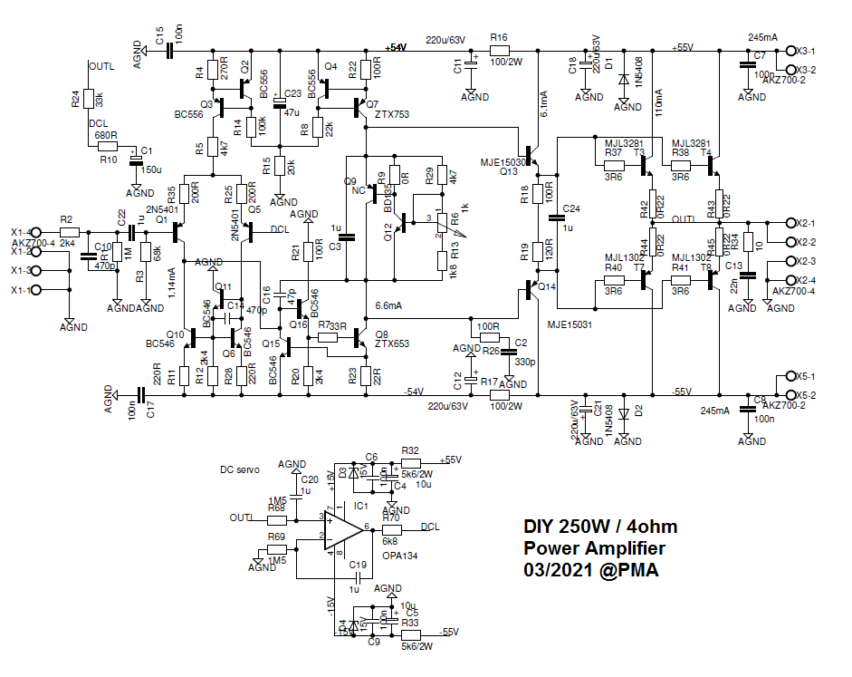
This is the complete schematics of the amplifier that I built
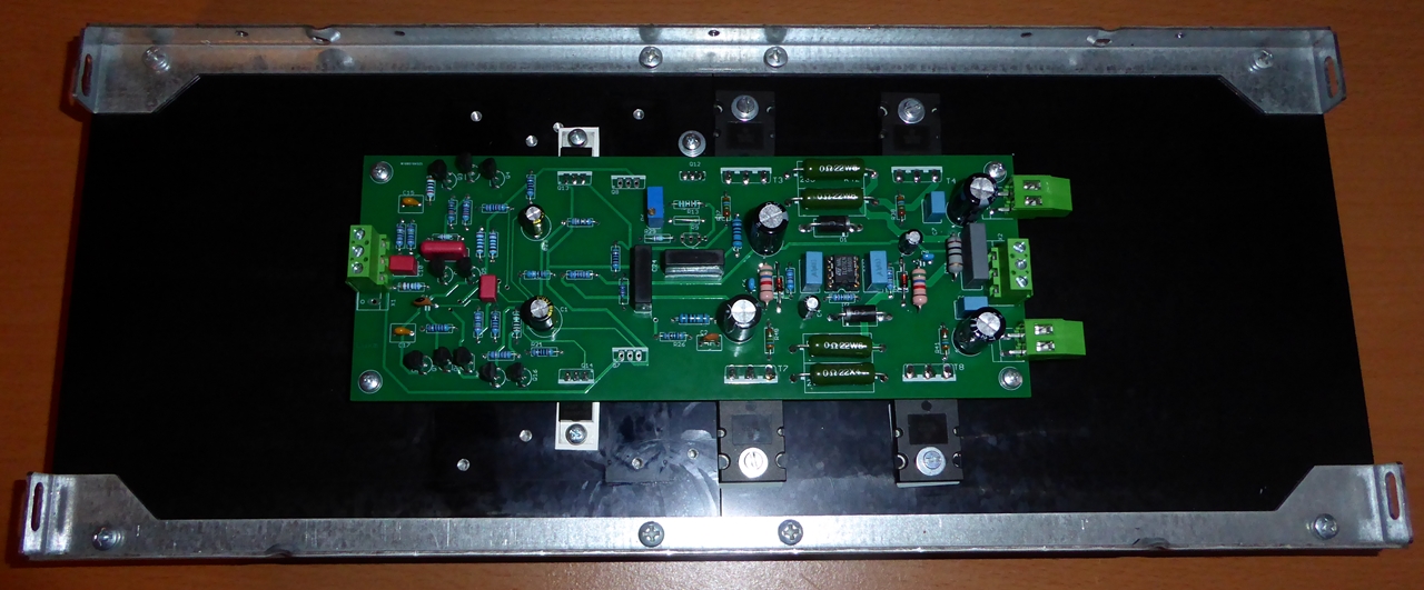
It was built into my prototype case, which determined the size of the PCB and also components placement and drilling. The case is 19” 4U, dimensions 450 x 415 x 180 mm. It has big side heatsinks and can accommodate two 300VA toroidal transformers, that are needed for the dual-mono 2x250W amplifier concept with long-term full-power capacity.
This is the amplifier PCB mounted on the heatsink
and this is the amplifier board in the prototype 19” 4U case (the bottom board. The top board is a CFA amp - it will be replaced soon)
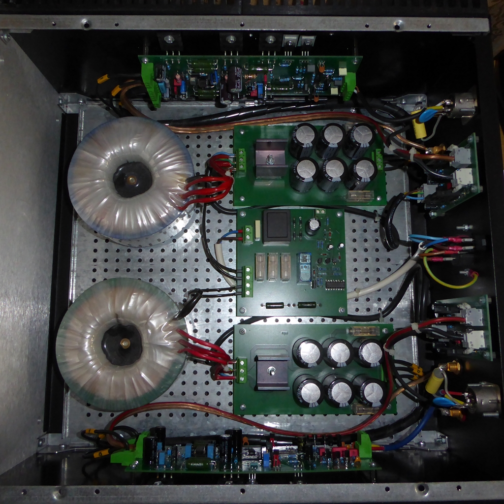
There are two transformers, two rectifier-filter boards, two amplifier boards and two DC protection SSR boards inside the case. The metal case is grounded (connected to PE) but the signal grounds of the left and right channels are connected to the case through the Rth//C components, to prevent usual serious ground-loop hum issues. The design is dual-mono and the signal grounds of the left and right channels are not directly interconnected.
Two MJL3281/1302 output pairs make 250W/4ohm power possible with respect to SOA (Safe Operating Area) of the transistors. It is possible to use speaker/complex load that does not fall below 4 ohm in its impedance/frequency plot. The worst case simulation with the load that well reflects the woofer impedance shows that the SOA I/V trajectory of one output device is just at the edge.
This is the impedance response used in the simulation
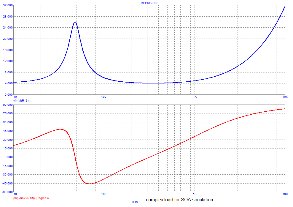
and this is the SOA simulation for 1 power transistor, with dummy load impedance schematics
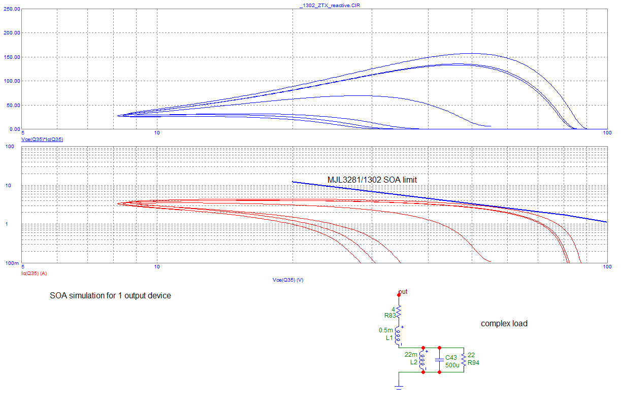
Interestingly enough the amp may drive purely resistive load of 2 ohm up to full output swing and still stay inside allowed SOA boundaries. It only tells that pure resistive loads are inadequate for both simulation and testing and do not reflect real-world speaker load.
Another interesting points of the schematics are the Q16 emitter follower (beta enhancer) that greatly reduces VAS distortion and increases open loop gain and all the current sources that improve PSR (ripple rejection).
Functional sample parameters
Measurements
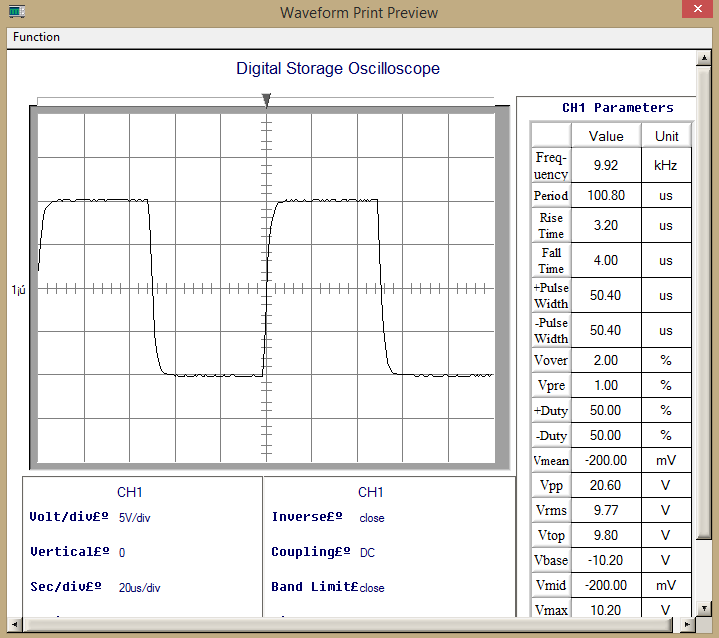
Response to 10kHz square wave
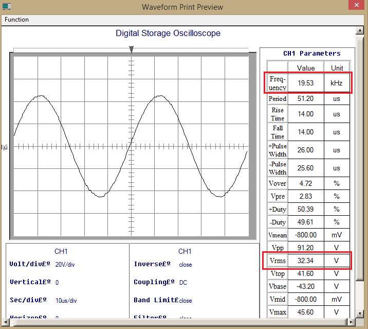
Sine 20kHz at full power into 4ohm load
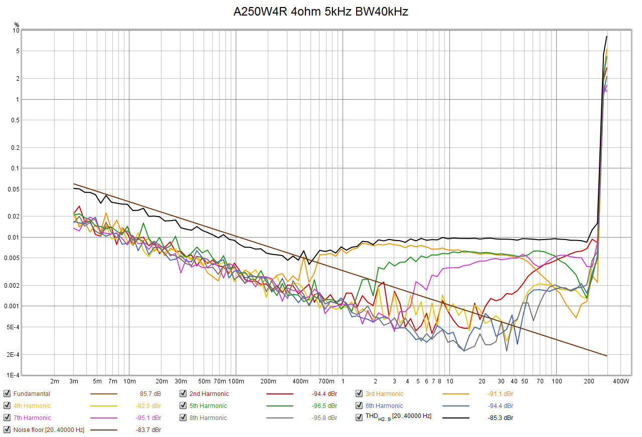
Distortion measurements - as mentioned in post #25, the soundcard originally used had H2 distortion similar as this amplifier so there happened a distortion cancellation in some measurements. These measurements have already been replaced by valid ones.
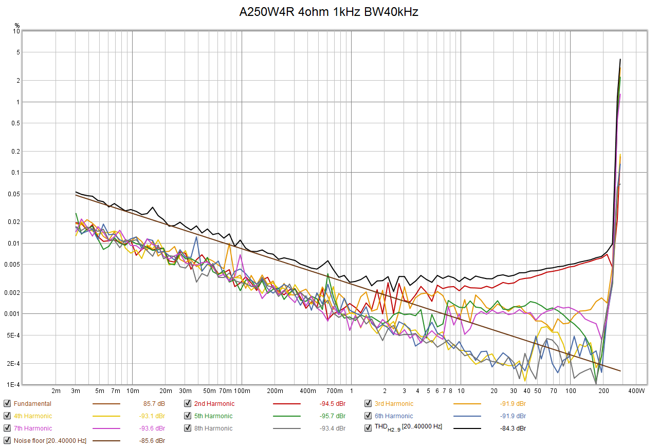
THD vs. output power into 4ohm load at 1kHz BW40kHz
THD vs. output power into 4ohm at 5kHz BW40kHz
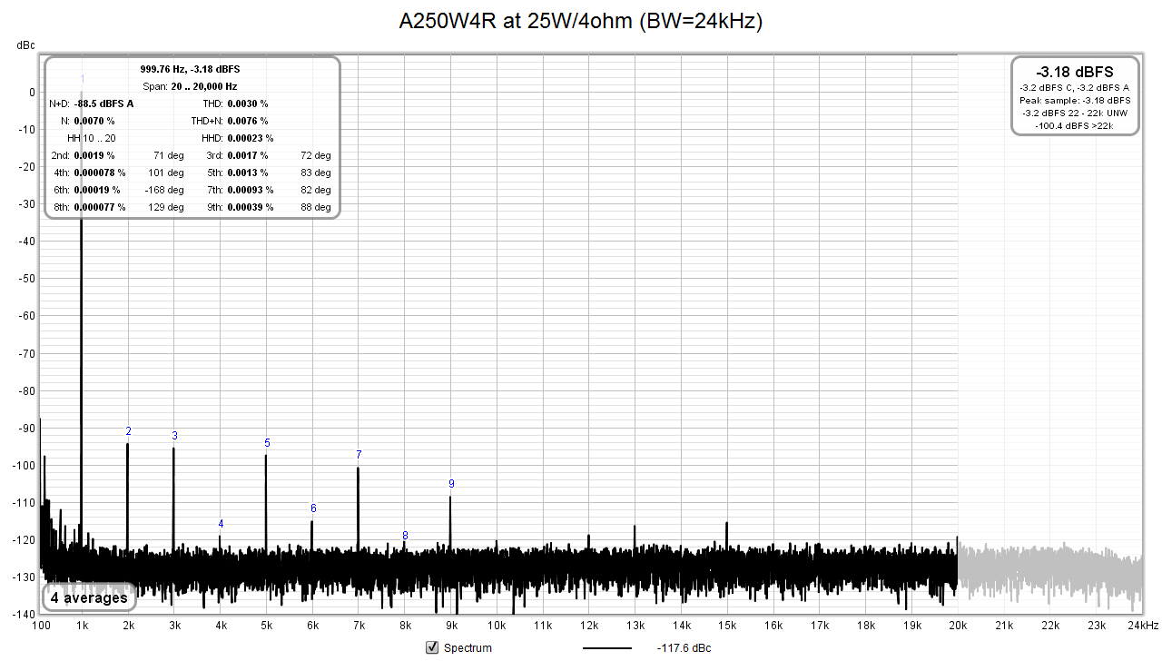
THD 1kHz spectrum at 25W/4ohm/1kHz
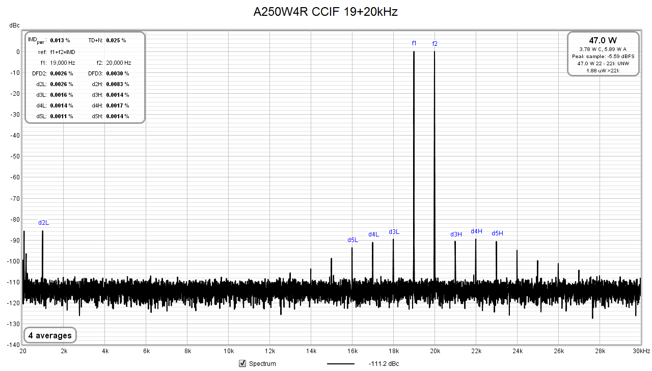
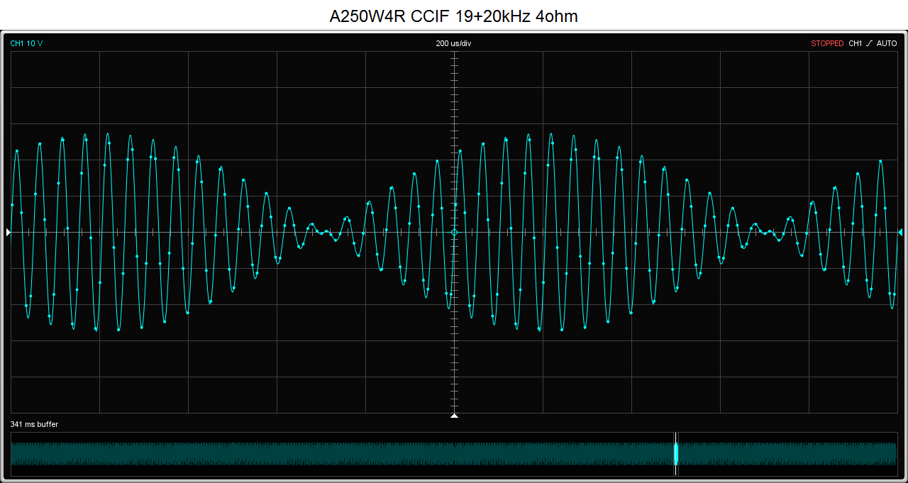
CCIF IMD 19+20kHz at 56Vp-p/4ohm
Conclusion
The amp looks promising. Just one channel has been built at the moment. I will make a second board and then make some listening tests as well.
Hello all, the thread posted here by @sabristol
https://www.audiosciencereview.com/forum/index.php?threads/luxman-l-85v-integrated-amplifier.20657/
inspired me to build a new DIY amplifier functional sample. The circuit posted in the link above is called “Luxman L-85” but in fact the topology is rather the Douglas Self's “Blameless Amplifier” discussed in his book Audio Power Amplifier Design Handbook on also on his website
http://www.douglas-self.com/ampins/dipa/dipa.htm
http://www.douglas-self.com/ampins/dipa/dpafig33.gif
The original Luxman PB-1037 main amplifier circuit is more different with 2 differential stages instead of one, no use of EF VAS buffer etc.
@sabristol has made very good job in implementing improvements by Douglas Self (EF buffer before VAS etc.) and his circuit posted was a temptation to me to get even more power and less distortion from that circuit. The main change I made was to use 2 pairs of the output devices, to get more output current and power and less dependence on load impedance. I was thinking about my favorite and robust MJL21194/93 first but then decided to go for MJL3281/1302 pairs, which have even better linearity at high currents and are faster, though only very slightly weaker in SOA.
This is the complete schematics of the amplifier that I built
It was built into my prototype case, which determined the size of the PCB and also components placement and drilling. The case is 19” 4U, dimensions 450 x 415 x 180 mm. It has big side heatsinks and can accommodate two 300VA toroidal transformers, that are needed for the dual-mono 2x250W amplifier concept with long-term full-power capacity.
This is the amplifier PCB mounted on the heatsink
and this is the amplifier board in the prototype 19” 4U case (the bottom board. The top board is a CFA amp - it will be replaced soon)
There are two transformers, two rectifier-filter boards, two amplifier boards and two DC protection SSR boards inside the case. The metal case is grounded (connected to PE) but the signal grounds of the left and right channels are connected to the case through the Rth//C components, to prevent usual serious ground-loop hum issues. The design is dual-mono and the signal grounds of the left and right channels are not directly interconnected.
Two MJL3281/1302 output pairs make 250W/4ohm power possible with respect to SOA (Safe Operating Area) of the transistors. It is possible to use speaker/complex load that does not fall below 4 ohm in its impedance/frequency plot. The worst case simulation with the load that well reflects the woofer impedance shows that the SOA I/V trajectory of one output device is just at the edge.
This is the impedance response used in the simulation
and this is the SOA simulation for 1 power transistor, with dummy load impedance schematics
Interestingly enough the amp may drive purely resistive load of 2 ohm up to full output swing and still stay inside allowed SOA boundaries. It only tells that pure resistive loads are inadequate for both simulation and testing and do not reflect real-world speaker load.
Another interesting points of the schematics are the Q16 emitter follower (beta enhancer) that greatly reduces VAS distortion and increases open loop gain and all the current sources that improve PSR (ripple rejection).
Functional sample parameters
- input impedance ….. 70 kohm
- frequency range ….. 2Hz – 88kHz/-3dB
- full-power bandwidth ….. 20Hz – 20kHz
- output noise voltage A weighted ..... -84dBV(A)
- output power ….. 2x250W/4ohm for THD < 0.1% at 1kHz
- S/N at full power ..... 114dB(A)
- harmonic distortion ….. THD < 0.007% at 200W/4ohm/1kHz (see graphs)
- rise time of step response ….. 4us
- gain ….. 34.4dB
- dimensions ….. 450 x 415 x 180 mm
- weight ….. 30 kg approx.
- construction ….. dual-mono with 2 toroidal PSU transformers 300VA each
Measurements
Response to 10kHz square wave
Sine 20kHz at full power into 4ohm load
Distortion measurements - as mentioned in post #25, the soundcard originally used had H2 distortion similar as this amplifier so there happened a distortion cancellation in some measurements. These measurements have already been replaced by valid ones.
THD vs. output power into 4ohm load at 1kHz BW40kHz
THD vs. output power into 4ohm at 5kHz BW40kHz
THD 1kHz spectrum at 25W/4ohm/1kHz
CCIF IMD 19+20kHz at 56Vp-p/4ohm
Conclusion
The amp looks promising. Just one channel has been built at the moment. I will make a second board and then make some listening tests as well.
Last edited:
